SLASE86E June 2016 – December 2017 TAS2560
PRODUCTION DATA.
- 1 Features
- 2 Applications
- 3 Description
- 4 Revision History
- 5 Device Comparison Table
- 6 Pin Configuration and Functions
-
7 Specifications
- 7.1 Absolute Maximum Ratings
- 7.2 ESD Ratings
- 7.3 Recommended Operating Conditions
- 7.4 Thermal Information
- 7.5 Electrical Characteristics
- 7.6 I2C Timing Requirements
- 7.7 I2S/LJF/RJF Timing in Master Mode
- 7.8 I2S/LJF/RJF Timing in Slave Mode
- 7.9 DSP Timing in Master Mode
- 7.10 DSP Timing in Slave Mode
- 7.11 PDM Timing
- 7.12 Typical Characteristics
- 8 Parameter Measurement Information
-
9 Detailed Description
- 9.1 Overview
- 9.2 Functional Block Diagram
- 9.3
Feature Description
- 9.3.1 General I2C Operation
- 9.3.2 Single-Byte and Multiple-Byte Transfers
- 9.3.3 Single-Byte Write
- 9.3.4 Multiple-Byte Write and Incremental Multiple-Byte Write
- 9.3.5 Single-Byte Read
- 9.3.6 Multiple-Byte Read
- 9.3.7 PLL
- 9.3.8 Clock Distribution
- 9.3.9 Clock Error Detection
- 9.3.10 Class-D Edge Rate Control
- 9.3.11 IV Sense
- 9.3.12 Boost Control
- 9.3.13 Thermal Fold-back
- 9.3.14 Battery Guard AGC
- 9.3.15 Configurable Boost Current Limit (ILIM)
- 9.3.16 Fault Protection
- 9.3.17 Spread Spectrum vs Synchronized
- 9.3.18 IRQs and Flags
- 9.3.19 CRC checksum for I2C
- 9.3.20 PurePath Console 3 Software TAS2560 Application
- 9.4 Device Functional Modes
- 9.5 Operational Modes
- 9.6 Programming
- 9.7
Register Map
- 9.7.1 Register Map Summary
- 9.7.2 PAGE (book=0x00 page=0x00 address=0x00) [reset=0h]
- 9.7.3 RESET (book=0x00 page=0x00 address=0x01) [reset=0h]
- 9.7.4 MODE (book=0x00 page=0x00 address=0x02) [reset=1h]
- 9.7.5 SPK_CTRL (book=0x00 page=0x00 address=0x04) [reset=5Fh]
- 9.7.6 PWR_CTRL_2 (book=0x00 page=0x00 address=0x05) [reset=0h]
- 9.7.7 PWR_CTRL_1 (book=0x00 page=0x00 address=0x07) [reset=0h]
- 9.7.8 RAMP_CTRL (book=0x00 page=0x00 address=0x08) [reset=1h]
- 9.7.9 EDGE_ISNS_BOOST (book=0x00 page=0x00 address=0x09) [reset=83h]
- 9.7.10 PLL_CLKIN (book=0x00 page=0x00 address=0x0F) [reset=41h]
- 9.7.11 PLL_JVAL (book=0x00 page=0x00 address=0x10) [reset=4h]
- 9.7.12 PLL_DVAL_1 (book=0x00 page=0x00 address=0x11) [reset=0h]
- 9.7.13 PLL_DVAL_2 (book=0x00 page=0x00 address=0x12) [reset=0h]
- 9.7.14 ASI_FORMAT (book=0x00 page=0x00 address=0x14) [reset=2h]
- 9.7.15 ASI_CHANNEL (book=0x00 page=0x00 address=0x15) [reset=0h]
- 9.7.16 ASI_OFFSET_1 (book=0x00 page=0x00 address=0x16) [reset=0h]
- 9.7.17 ASI_OFFSET_2 (book=0x00 page=0x00 address=0x17) [reset=0h]
- 9.7.18 ASI_CFG_1 (book=0x00 page=0x00 address=0x18) [reset=0h]
- 9.7.19 ASI_DIV_SRC (book=0x00 page=0x00 address=0x19) [reset=0h]
- 9.7.20 ASI_BDIV (book=0x00 page=0x00 address=0x1A) [reset=1h]
- 9.7.21 ASI_WDIV (book=0x00 page=0x00 address=0x1B) [reset=40h]
- 9.7.22 PDM_CFG (book=0x00 page=0x00 address=0x1C) [reset=0h]
- 9.7.23 PDM_DIV (book=0x00 page=0x00 address=0x1D) [reset=8h]
- 9.7.24 DSD_DIV (book=0x00 page=0x00 address=0x1E) [reset=8h]
- 9.7.25 CLK_ERR_1 (book=0x00 page=0x00 address=0x21) [reset=3h]
- 9.7.26 CLK_ERR_2 (book=0x00 page=0x00 address=0x22) [reset=3Fh]
- 9.7.27 IRQ_PIN_CFG (book=0x00 page=0x00 address=0x23) [reset=21h]
- 9.7.28 INT_CFG_1 (book=0x00 page=0x00 address=0x24) [reset=0h]
- 9.7.29 INT_CFG_2 (book=0x00 page=0x00 address=0x25) [reset=0h]
- 9.7.30 INT_DET_1 (book=0x00 page=0x00 address=0x26) [reset=0h]
- 9.7.31 INT_DET_2 (book=0x00 page=0x00 address=0x27) [reset=0h]
- 9.7.32 STATUS_POWER (book=0x00 page=0x00 address=0x2A) [reset=0h]
- 9.7.33 SAR_VBAT_MSB (book=0x00 page=0x00 address=0x2D) [reset=C0h]
- 9.7.34 SAR_VBAT_LSB (book=0x00 page=0x00 address=0x2E) [reset=0h]
- 9.7.35 DIE_TEMP_SENSOR (book=0x00 page=0x00 address=0x31) [reset=0h]
- 9.7.36 LOW_PWR_MODE (book=0x00 page=0x00 address=0x35) [reset=0h]
- 9.7.37 PCM_RATE (book=0x00 page=0x00 address=0x36) [reset=32h]
- 9.7.38 CLOCK_ERR_CFG_1 (book=0x00 page=0x00 address=0x4F) [reset=0h]
- 9.7.39 CLOCK_ERR_CFG_2 (book=0x00 page=0x00 address=0x50) [reset=11h]
- 9.7.40 PROTECTION_CFG_1 (book=0x00 page=0x00 address=0x58) [reset=3h]
- 9.7.41 CRC_CHECKSUM (book=0x00 page=0x00 address=0x7E) [reset=0h]
- 9.7.42 BOOK (book=0x00 page=0x00 address=0x7F) [reset=0h]
- 10Application and Implementation
- 11Power Supply Recommendations
- 12Layout
- 13Device and Documentation Support
- 14Mechanical, Packaging, and Orderable Information
Package Options
Refer to the PDF data sheet for device specific package drawings
Mechanical Data (Package|Pins)
- YFF|30
Thermal pad, mechanical data (Package|Pins)
Orderable Information
10 Application and Implementation
NOTE
Information in the following applications sections is not part of the TI component specification, and TI does not warrant its accuracy or completeness. TI’s customers are responsible for determining suitability of components for their purposes. Customers should validate and test their design implementation to confirm system functionality.
10.1 Application Information
The TAS2560 is a digital or analog input high efficiency Class-D audio power amplifier with advanced battery current management and an integrated Class-H boost converter. In auto passthrough mode, the Class-H boost converter generates the Class-D amplifier supply rail. During low Class-D output power, the boost improves efficiency by deactivating and connecting VBAT directly to the Class-D amplifier supply. When high power audio is required, the boost quickly activates to provide louder audio than a stand-alone amplifier connected directly to the battery. To enable load monitoring, the TAS2560 constantly measures the current and voltage across the load and provides a digital stream of this information back to a processor.
10.2 Typical Applications
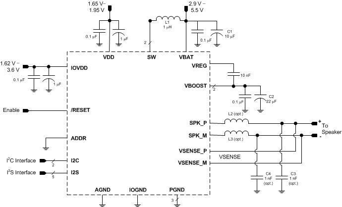
 Figure 98. Typical Application - Digital Audio Input
Table 101. Recommended External Components
| COMPONENT | DESCRIPTION | SPECIFICATION | MIN | TYP | MAX | UNIT |
|---|---|---|---|---|---|---|
| L1 | Boost Converter Inductor(1) | Inductance, 20% Tolerance | 1 | 1 | µH | |
| Saturation Current | 3.1 | A | ||||
| L2, L3 | EMI Filter Inductors (optional). These are not recommended as it degrades THD+N performance. TAS2560 is a filter-less Class-D and does not require these bead inductors. | Impedance at 100 MHz | 120 | O | ||
| DC Resistance | 0.095 | O | ||||
| DC Current | 2 | A | ||||
| Size | 0402 | EIA | ||||
| C1 | Boost Converter Input Capacitor(1) | Capacitance, 20% Tolerance | 10 | µF | ||
| C2 | Boost Converter Output Capacitor | Type | X5R | |||
| Capacitance, 20% Tolerance | 22 | 47 | µF | |||
| Rated Voltage | 16 | V | ||||
| Capacitance at 8.5 V derating | 3.3 | µF | ||||
| C3, C4 | EMI Filter Capacitors (optional, must use L2, L3 if C3, C4 used) | Capacitance | 1 | nF |
10.2.1 Design Requirements
For this design example, use the parameters shown in Table 102.
Table 102. Design Parameters
| DESIGN PARAMETER | EXAMPLE VALUE |
|---|---|
| Audio Input | Digital Audio, I2S |
| Current and Voltage Data Stream | Digital Audio, I2S |
| Mono or Stereo Configuration | Mono |
| Max Output Power at 1% THD+N | 3.8 W |
10.2.1.1 Detailed Design Procedure
10.2.1.1.1 Mono/Stereo Configuration
In this application, the device is assumed to be operating in mono mode. See General I2C Operation for information on changing the I2C address of the TAS2560 to support stereo operation. Mono or stereo configuration does not impact the device performance.
10.2.1.1.2 Boost Converter Passive Devices
The boost converter requires three passive devices that are labeled L1, C1 and C2 in Figure 98 and whose specifications are provided in Table 101. These specifications are based on the design of the TAS2560 and are necessary to meet the performance targets of the device. In particular, L1 should not be allowed to enter in the current saturation region. The saturation current for L1 should be > ILIM to deliver Class-D peak power.
Additionally, the ratio of L1/C2 (the derated value of C2 at 8.5 V should be used in this ratio) has to be lesser than 1/3 for boost stability. This 1/3 ratio should be maintained including the worst case variation of L1 and C2. To satisfy sufficient energy transfer, L1 needs to be ≥ 1 μH at the boost switching frequency (approximately 1.7 MHz). Using a 1 μH will have more boost ripple than a 2.2 μH but the PSRR should minimize the effect from the additional ripple. Finally, the minimum C2 (derated value at 8.5 V) should be > 3.3 μF for Class-D power delivery specification.
10.2.1.1.3 EMI Passive Devices
The TAS2560 supports edge-rate control to minimize EMI, but the system designer may want to include passive devices on the Class-D output devices. These passive devices that are labeled L2, L3, C3 and C4 in Figure 98 and their recommended specifications are provided in Table 101. If C3 and C4 are used, they must be placed after L2 and L3 respectively to maintain the stability of the output stage.
10.2.1.1.4 Miscellaneous Passive Devices
- VREG Capacitor: Needs to be 10 nF to meet boost and Class-D power delivery and efficiency specs.
10.2.2 Application Performance Plots

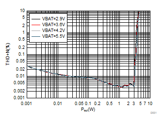
| Freq = 1kHz VBAT = 3.6 V, AVDD = IOVDD = 1.8 V, RESETZ = IOVDD, RL = 8 Ω + 33 µH, I2S digital input, Mode 1 |
10.3 Initialization Set Up
To configure the TAS2560, follow these steps.
- Bring-up the power supplies as in Power Supply Sequencing.
- Set the RESETZ terminal to HIGH.
- Follow the software sequence in the Programming section.