SLASEG8A March 2016 – July 2017 TAS5782M
PRODUCTION DATA.
- 1 Features
- 2 Applications
- 3 Description
- 4 Revision History
- 5 Device Comparison Table
- 6 Pin Configuration and Functions
-
7 Specifications
- 7.1 Absolute Maximum Ratings
- 7.2 ESD Ratings
- 7.3 Recommended Operating Conditions
- 7.4 Thermal Information
- 7.5 Electrical Characteristics
- 7.6 Power Dissipation Characteristics
- 7.7 MCLK Timing
- 7.8 Serial Audio Port Timing - Slave Mode
- 7.9 Serial Audio Port Timing - Master Mode
- 7.10 I2C Bus Timing - Standard
- 7.11 I2C Bus Timing - Fast
- 7.12 SPK_MUTE Timing
- 7.13 Typical Characteristics
- 8 Parametric Measurement Information
-
9 Detailed Description
- 9.1 Overview
- 9.2 Functional Block Diagram
- 9.3
Feature Description
- 9.3.1 Power-on-Reset (POR) Function
- 9.3.2 Device Clocking
- 9.3.3
Serial Audio Port
- 9.3.3.1 Clock Master Mode from Audio Rate Master Clock
- 9.3.3.2 Clock Master from a Non-Audio Rate Master Clock
- 9.3.3.3 Clock Slave Mode with 4-Wire Operation (SCLK, MCLK, LRCK/FS, SDIN)
- 9.3.3.4 Clock Slave Mode with SCLK PLL to Generate Internal Clocks (3-Wire PCM)
- 9.3.3.5 Serial Audio Port - Data Formats and Bit Depths
- 9.3.3.6 Input Signal Sensing (Power-Save Mode)
- 9.3.4 Enable Device
- 9.3.5 Volume Control
- 9.3.6 Adjustable Amplifier Gain and Switching Frequency Selection
- 9.3.7
Error Handling and Protection Suite
- 9.3.7.1 Device Overtemperature Protection
- 9.3.7.2 SPK_OUTxx Overcurrent Protection
- 9.3.7.3 DC Offset Protection
- 9.3.7.4 Internal VAVDD Undervoltage-Error Protection
- 9.3.7.5 Internal VPVDD Undervoltage-Error Protection
- 9.3.7.6 Internal VPVDD Overvoltage-Error Protection
- 9.3.7.7 External Undervoltage-Error Protection
- 9.3.7.8 Internal Clock Error Notification (CLKE)
- 9.3.8 GPIO Port and Hardware Control Pins
- 9.3.9 I2C Communication Port
- 9.4 Device Functional Modes
- 10Application and Implementation
- 11Power Supply Recommendations
- 12Layout
-
13Register Maps
- 13.1
Registers - Page 0
- 13.1.1 Register 1 (0x01)
- 13.1.2 Register 6 (0x06)
- 13.1.3 Register 7 (0x07)
- 13.1.4 Register 8 (0x08)
- 13.1.5 Register 9 (0x09)
- 13.1.6 Register 12 (0x0C)
- 13.1.7 Register 13 (0x0D)
- 13.1.8 Register 14 (0x0E)
- 13.1.9 Register 15 (0x0F)
- 13.1.10 Register 16 (0x10)
- 13.1.11 Register 17 (0x11)
- 13.1.12 Register 18 (0x12)
- 13.1.13 Register 20 (0x14)
- 13.1.14 Register 21 (0x15)
- 13.1.15 Register 22 (0x16)
- 13.1.16 Register 23 (0x17)
- 13.1.17 Register 24 (0x18)
- 13.1.18 Register 27 (0x1B)
- 13.1.19 Register 28 (0x1C)
- 13.1.20 Register 29 (0x1D)
- 13.1.21 Register 30 (0x1E)
- 13.1.22 Register 32 (0x20)
- 13.1.23 Register 33 (0x21)
- 13.1.24 Register 34 (0x22)
- 13.1.25 Register 37 (0x25)
- 13.1.26 Register 40 (0x28)
- 13.1.27 Register 41 (0x29)
- 13.1.28 Register 42 (0x2A)
- 13.1.29 Register 43 (0x2B)
- 13.1.30 Register 44 (0x2C)
- 13.1.31 Register 59 (0x3B)
- 13.1.32 Register 60 (0x3C)
- 13.1.33 Register 61 (0x3D)
- 13.1.34 Register 62 (0x3E)
- 13.1.35 Register 63 (0x3F)
- 13.1.36 Register 64 (0x40)
- 13.1.37 Register 65 (0x41)
- 13.1.38 Register 67 (0x43)
- 13.1.39 Register 68 (0x44)
- 13.1.40 Register 69 (0x45)
- 13.1.41 Register 70 (0x46)
- 13.1.42 Register 71 (0x47)
- 13.1.43 Register 72 (0x48)
- 13.1.44 Register 73 (0x49)
- 13.1.45 Register 74 (0x4A)
- 13.1.46 Register 75 (0x4B)
- 13.1.47 Register 76 (0x4C)
- 13.1.48 Register 78 (0x4E)
- 13.1.49 Register 79 (0x4F)
- 13.1.50 Register 83 (0x53)
- 13.1.51 Register 85 (0x55)
- 13.1.52 Register 86 (0x56)
- 13.1.53 Register 87 (0x57)
- 13.1.54 Register 88 (0x58)
- 13.1.55 Register 91 (0x5B)
- 13.1.56 Register 92 (0x5C)
- 13.1.57 Register 93 (0x5D)
- 13.1.58 Register 94 (0x5E)
- 13.1.59 Register 95 (0x5F)
- 13.1.60 Register 108 (0x6C)
- 13.1.61 Register 119 (0x77)
- 13.1.62 Register 120 (0x78)
- 13.2 Registers - Page 1
- 13.1
Registers - Page 0
- 14Device and Documentation Support
- 15Mechanical, Packaging, and Orderable Information
Package Options
Mechanical Data (Package|Pins)
- DCA|48
Thermal pad, mechanical data (Package|Pins)
- DCA|48
Orderable Information
6 Pin Configuration and Functions
DCA Package
48-Pin TSSOP with PowerPAD™
Top View
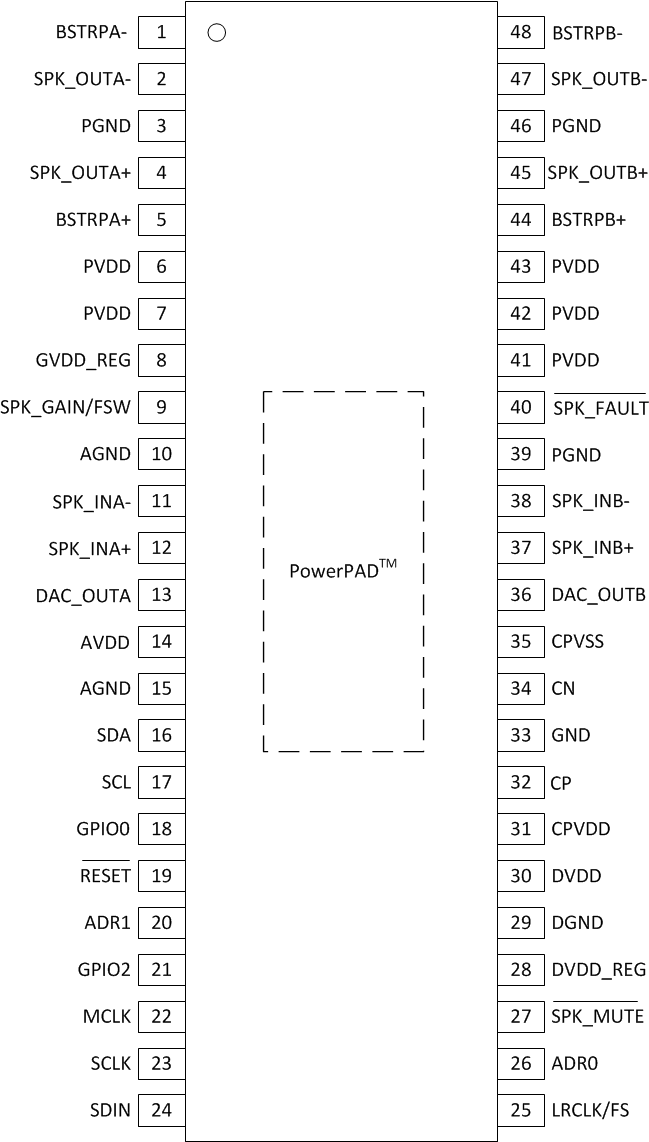
Pin Functions
| PIN | TYPE(1) | INTERNAL TERMINATION | DESCRIPTION | |
|---|---|---|---|---|
| NAME | NO. | |||
| ADR0 | 26 | DI | Sets the LSB of the I2C address to 0 if pulled to GND, to 1 if pulled to DVDD | |
| ADR1 | 20 | DI | Sets the second LSB of the I2C address to 0 if pulled to GND, to 1 if pulled to DVDD | |
| AGND | 10 | G | — | Ground reference for analog circuitry(2) |
| 15 | ||||
| AVDD | 14 | P | Figure 2 | Power supply for internal analog circuitry |
| BSTRPA– | 1 | P | Figure 3 | Connection point for the SPK_OUTA– bootstrap capacitor which is used to create a power supply for the high-side gate drive for SPK_OUTA– |
| BSTRPA+ | 5 | P | Connection point for the SPK_OUTA+ bootstrap capacitor which is used to create a power supply for the high-side gate drive for SPK_OUTA+ | |
| BSTRPB– | 48 | P | Connection point for the SPK_OUTB– bootstrap capacitor which is used to create a power supply for the high-side gate drive for SPK_OUTB– | |
| BSTRPB+ | 44 | P | Connection point for the SPK_OUTB+ bootstrap capacitor which is used to create a power supply for the high-side gate drive for SPK_OUTB+ | |
| CN | 34 | P | Figure 14 | Negative pin for capacitor connection used in the line-driver charge pump |
| CP | 32 | P | Figure 13 | Positive pin for capacitor connection used in the line-driver charge pump |
| CPVDD | 31 | P | Figure 2 | Power supply for charge pump circuitry |
| CPVSS | 35 | P | Figure 14 | –3.3-V supply generated by charge pump for the DAC |
| DAC_OUTA | 13 | AO | Figure 8 | Single-ended output for Channel A of the DAC |
| DAC_OUTB | 36 | AO | Single-ended output for Channel B of the DAC | |
| DGND | 29 | G | — | Ground reference for digital circuitry. Connect this pin to the system ground. |
| DVDD | 30 | P | Figure 2 | Power supply for the internal digital circuitry |
| DVDD_REG | 28 | P | Figure 15 | Voltage regulator derived from DVDD supply for use for internal digital circuitry. This pin is provided as a connection point for filtering capacitors for this supply and must not be used to power any external circuitry. |
| GND | 33 | G | — | Ground pin for device. This pin should be connected to the system ground. |
| GPIO0 | 18 | DI/O | General purpose input/output pins (GPIOx). Refer to GPIO registers for configuration. | |
| GPIO2 | 21 | |||
| GVDD_REG | 8 | P | Figure 5 | Voltage regulator derived from PVDD supply to generate the voltage required for the gate drive of output MOSFETs. This pin is provided as a connection point for filtering capacitors for this supply and must not be used to power any external circuitry. |
| LRCK/FS | 25 | DI/O | Figure 11 | Word select clock for the digital signal that is active on the serial port's input data line. In I2S, LJ, and RJ, this corresponds to the left channel and right channel boundary. In TDM mode, this corresponds to the frame sync boundary. |
| MCLK | 22 | DI | Master clock used for internal clock tree and sub-circuit and state machine clocking | |
| PGND | 3 | G | — | Ground reference for power device circuitry. Connect this pin to the system ground. |
| 39 | ||||
| 46 | ||||
| PVDD | 6 | P | Figure 1 | Power supply for internal power circuitry |
| 7 | ||||
| 41 | ||||
| 42 | ||||
| 43 | ||||
| RESET | 19 | DI | Figure 17 | Device reset input. Pull down to reset, pull up to activate device. |
| SCL | 17 | DI | Figure 10 | I2C serial control port clock |
| SCLK | 23 | DI/O | Figure 11 | Bit clock for the digital signal that is active on the input data line of the serial data port |
| SDA | 16 | DI/O | Figure 9 | I2C serial control port data |
| SDIN | 24 | D1 | Figure 11 | Data line to the serial data port |
| SPK_INA– | 11 | AI | Figure 7 | Negative pin for differential speaker amplifier input A |
| SPK_INA+ | 12 | AI | Positive pin for differential speaker amplifier input A | |
| SPK_INB– | 38 | AI | Negative pin for differential speaker amplifier input B | |
| SPK_INB+ | 37 | AI | Positive pin for differential speaker amplifier input B | |
| SPK_FAULT | 40 | DO | Figure 16 | Fault pin which is pulled low when an overcurrent, overtemperature, or DC detect fault occurs |
| SPK_GAIN/FREQ | 9 | AI | Figure 6 | Sets the gain and switching frequency of the speaker amplifier, latched in upon start-up of the device. |
| SPK_OUTA– | 2 | AO | Figure 4 | Negative pin for differential speaker amplifier output A |
| SPK_OUTA+ | 4 | AO | Positive pin for differential speaker amplifier output A | |
| SPK_OUTB– | 47 | AO | Negative pin for differential speaker amplifier output B | |
| SPK_OUTB+ | 45 | AO | Positive pin for differential speaker amplifier output B | |
| SPK_MUTE | 27 | I | Figure 12 | Speaker amplifier mute which must be pulled low (connected to DGND) to mute the device and pulled high (connected to DVDD) to unmute the device. |
| PowerPAD | — | G | — | Provides both electrical and thermal connection from the device to the board. A matching ground pad must be provided on the PCB and the device connected to it through solder. For proper electrical operation, this ground pad must be connected to the system ground. |
(1) AI = Analog input, AO = Analog output, DI = Digital Input, DO = Digital Output, DI/O = Digital Bi-directional (input and output), P = Power, G = Ground (0 V)
(2) This pin should be connected to the system ground.
6.1 Internal Pin Configurations
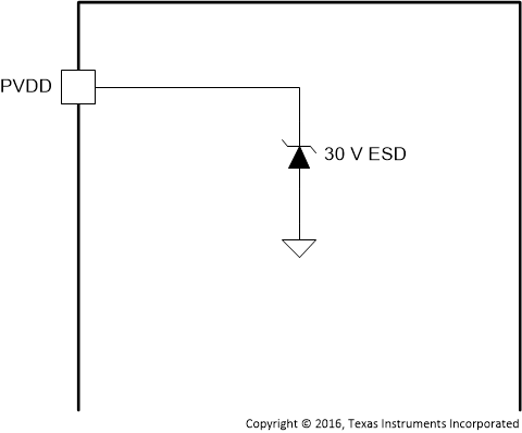 Figure 1. PVDD Pins
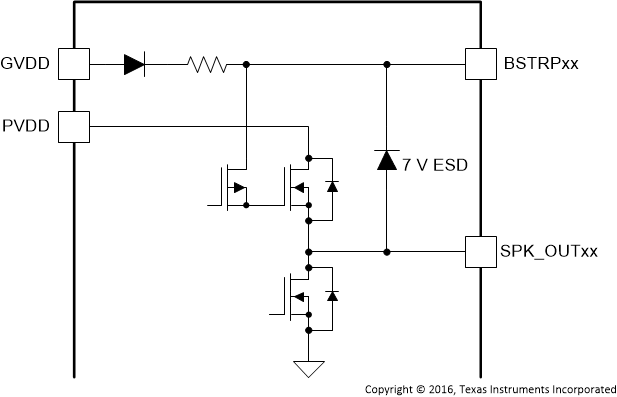 Figure 3. BSTRPxx Pins
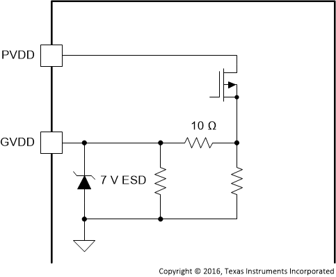 Figure 5. GVDD_REG Pin
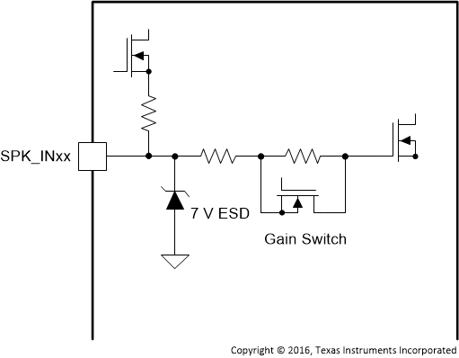 Figure 7. SPK_INxx Pins
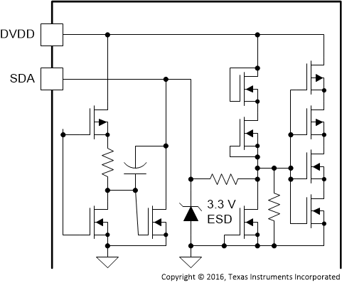 Figure 9. SDA Pin
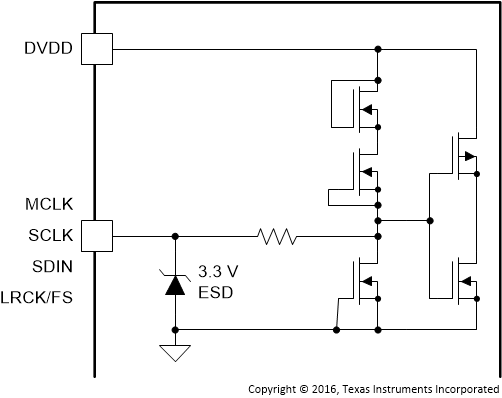 Figure 11. SCLK, MCLK, SDIN, and LRCK/FS Pins
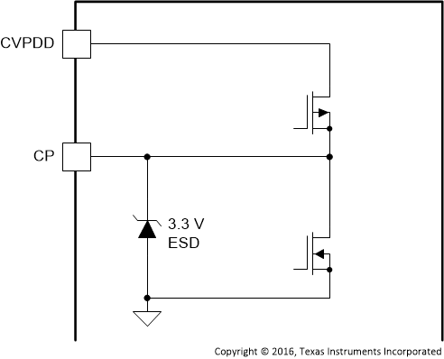 Figure 13. CP Pin
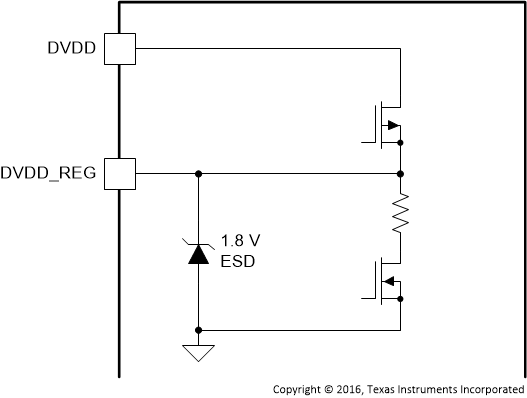 Figure 15. DVDD_REG Pin
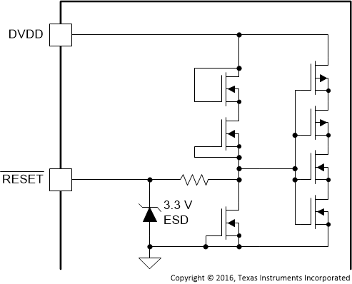 Figure 17. RESET Pin
 Figure 2. AVDD, DVDD and CPVDD Pins
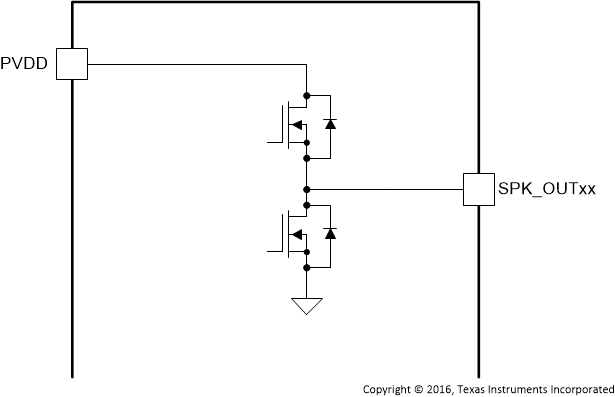 Figure 4. SPK_OUTxx Pins
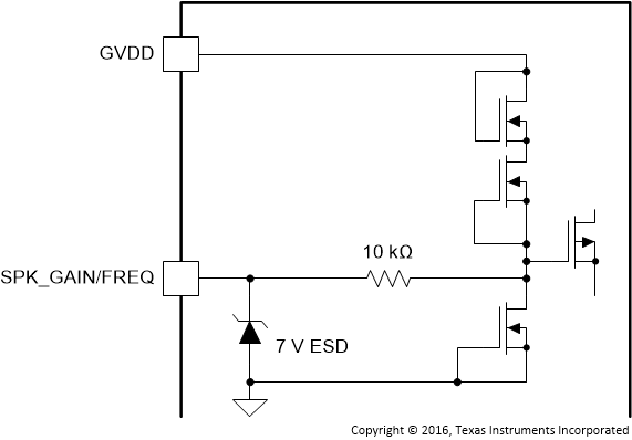 Figure 6. SPK_GAIN/FREQ Pin
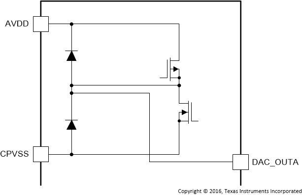 Figure 8. DAC_OUTx Pins
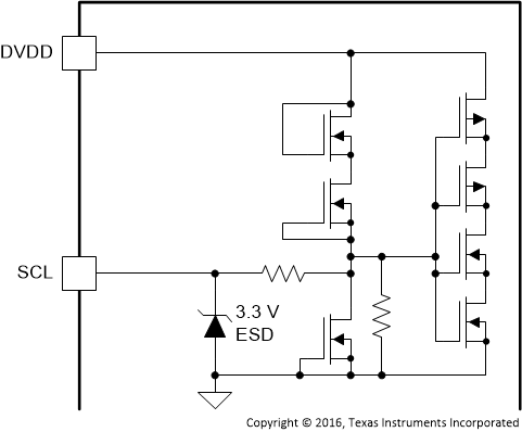 Figure 10. SCL Pin
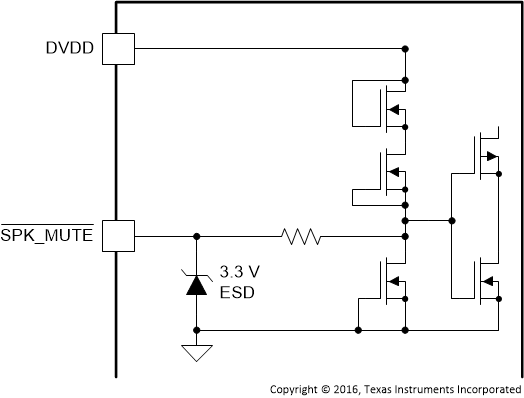 Figure 12. SPK_MUTE Pin
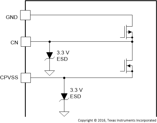 Figure 14. CN and CPVSS Pins
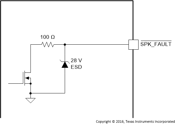 Figure 16. SPK_FAULT Pin