SLASEG8A March 2016 – July 2017 TAS5782M
PRODUCTION DATA.
- 1 Features
- 2 Applications
- 3 Description
- 4 Revision History
- 5 Device Comparison Table
- 6 Pin Configuration and Functions
-
7 Specifications
- 7.1 Absolute Maximum Ratings
- 7.2 ESD Ratings
- 7.3 Recommended Operating Conditions
- 7.4 Thermal Information
- 7.5 Electrical Characteristics
- 7.6 Power Dissipation Characteristics
- 7.7 MCLK Timing
- 7.8 Serial Audio Port Timing - Slave Mode
- 7.9 Serial Audio Port Timing - Master Mode
- 7.10 I2C Bus Timing - Standard
- 7.11 I2C Bus Timing - Fast
- 7.12 SPK_MUTE Timing
- 7.13 Typical Characteristics
- 8 Parametric Measurement Information
-
9 Detailed Description
- 9.1 Overview
- 9.2 Functional Block Diagram
- 9.3
Feature Description
- 9.3.1 Power-on-Reset (POR) Function
- 9.3.2 Device Clocking
- 9.3.3
Serial Audio Port
- 9.3.3.1 Clock Master Mode from Audio Rate Master Clock
- 9.3.3.2 Clock Master from a Non-Audio Rate Master Clock
- 9.3.3.3 Clock Slave Mode with 4-Wire Operation (SCLK, MCLK, LRCK/FS, SDIN)
- 9.3.3.4 Clock Slave Mode with SCLK PLL to Generate Internal Clocks (3-Wire PCM)
- 9.3.3.5 Serial Audio Port - Data Formats and Bit Depths
- 9.3.3.6 Input Signal Sensing (Power-Save Mode)
- 9.3.4 Enable Device
- 9.3.5 Volume Control
- 9.3.6 Adjustable Amplifier Gain and Switching Frequency Selection
- 9.3.7
Error Handling and Protection Suite
- 9.3.7.1 Device Overtemperature Protection
- 9.3.7.2 SPK_OUTxx Overcurrent Protection
- 9.3.7.3 DC Offset Protection
- 9.3.7.4 Internal VAVDD Undervoltage-Error Protection
- 9.3.7.5 Internal VPVDD Undervoltage-Error Protection
- 9.3.7.6 Internal VPVDD Overvoltage-Error Protection
- 9.3.7.7 External Undervoltage-Error Protection
- 9.3.7.8 Internal Clock Error Notification (CLKE)
- 9.3.8 GPIO Port and Hardware Control Pins
- 9.3.9 I2C Communication Port
- 9.4 Device Functional Modes
- 10Application and Implementation
- 11Power Supply Recommendations
- 12Layout
-
13Register Maps
- 13.1
Registers - Page 0
- 13.1.1 Register 1 (0x01)
- 13.1.2 Register 6 (0x06)
- 13.1.3 Register 7 (0x07)
- 13.1.4 Register 8 (0x08)
- 13.1.5 Register 9 (0x09)
- 13.1.6 Register 12 (0x0C)
- 13.1.7 Register 13 (0x0D)
- 13.1.8 Register 14 (0x0E)
- 13.1.9 Register 15 (0x0F)
- 13.1.10 Register 16 (0x10)
- 13.1.11 Register 17 (0x11)
- 13.1.12 Register 18 (0x12)
- 13.1.13 Register 20 (0x14)
- 13.1.14 Register 21 (0x15)
- 13.1.15 Register 22 (0x16)
- 13.1.16 Register 23 (0x17)
- 13.1.17 Register 24 (0x18)
- 13.1.18 Register 27 (0x1B)
- 13.1.19 Register 28 (0x1C)
- 13.1.20 Register 29 (0x1D)
- 13.1.21 Register 30 (0x1E)
- 13.1.22 Register 32 (0x20)
- 13.1.23 Register 33 (0x21)
- 13.1.24 Register 34 (0x22)
- 13.1.25 Register 37 (0x25)
- 13.1.26 Register 40 (0x28)
- 13.1.27 Register 41 (0x29)
- 13.1.28 Register 42 (0x2A)
- 13.1.29 Register 43 (0x2B)
- 13.1.30 Register 44 (0x2C)
- 13.1.31 Register 59 (0x3B)
- 13.1.32 Register 60 (0x3C)
- 13.1.33 Register 61 (0x3D)
- 13.1.34 Register 62 (0x3E)
- 13.1.35 Register 63 (0x3F)
- 13.1.36 Register 64 (0x40)
- 13.1.37 Register 65 (0x41)
- 13.1.38 Register 67 (0x43)
- 13.1.39 Register 68 (0x44)
- 13.1.40 Register 69 (0x45)
- 13.1.41 Register 70 (0x46)
- 13.1.42 Register 71 (0x47)
- 13.1.43 Register 72 (0x48)
- 13.1.44 Register 73 (0x49)
- 13.1.45 Register 74 (0x4A)
- 13.1.46 Register 75 (0x4B)
- 13.1.47 Register 76 (0x4C)
- 13.1.48 Register 78 (0x4E)
- 13.1.49 Register 79 (0x4F)
- 13.1.50 Register 83 (0x53)
- 13.1.51 Register 85 (0x55)
- 13.1.52 Register 86 (0x56)
- 13.1.53 Register 87 (0x57)
- 13.1.54 Register 88 (0x58)
- 13.1.55 Register 91 (0x5B)
- 13.1.56 Register 92 (0x5C)
- 13.1.57 Register 93 (0x5D)
- 13.1.58 Register 94 (0x5E)
- 13.1.59 Register 95 (0x5F)
- 13.1.60 Register 108 (0x6C)
- 13.1.61 Register 119 (0x77)
- 13.1.62 Register 120 (0x78)
- 13.2 Registers - Page 1
- 13.1
Registers - Page 0
- 14Device and Documentation Support
- 15Mechanical, Packaging, and Orderable Information
Package Options
Mechanical Data (Package|Pins)
- DCA|48
Thermal pad, mechanical data (Package|Pins)
- DCA|48
Orderable Information
7 Specifications
7.1 Absolute Maximum Ratings
Free-air room temperature 25°C (unless otherwise noted)(1)| MIN | MAX | UNIT | ||
|---|---|---|---|---|
| DVDD, AVDD, CPVDD | Low-voltage digital, analog, charge pump supply | –0.3 | 3.9 | V |
| PVDD | PVDD supply | –0.3 | 30 | V |
| VI(AmpCtrl) | Input voltage for SPK_GAIN/FREQ and SPK_FAULT pins | –0.3 | VGVDD + 0.3 | V |
| VI(DigIn) | DVDD referenced digital inputs(2) | –0.5 | VDVDD + 0.5 | V |
| VI(SPK_INxx) | Analog input into speaker amplifier | –0.3 | 6.3 | V |
| VI(SPK_OUTxx) | Voltage at speaker output pins | –0.3 | 32 | V |
| Ambient operating temperature, TA | –25 | 85 | °C | |
| TJ | Operating junction temperature, digital die | –40 | 125 | °C |
| Operating junction temperature, power die | –40 | 165 | °C | |
| Tstg | Storage temperature | –40 | 125 | °C |
7.2 ESD Ratings
| VALUE | UNIT | |||
|---|---|---|---|---|
| V(ESD) | Electrostatic discharge | Human-body model (HBM), per ANSI/ESDA/JEDEC JS-001(1) | ±2000 | V |
| Charged-device model (CDM), per JEDEC specification JESD22-C101(2) | ±500 | |||
7.3 Recommended Operating Conditions
Free-air room temperature 25°C (unless otherwise noted)| MIN | NOM | MAX | UNIT | |||
|---|---|---|---|---|---|---|
| V(POWER) | Power supply inputs | DVDD, AVDD, CPVDD | 2.9 | 3.63 | V | |
| PVDD | 4.5 | 26.4 | ||||
| RSPK | Minimum speaker load | BTL Mode | 3 | Ω | ||
| PBTL Mode | 2 | Ω | ||||
| VIH(DigIn) | Input logic high for DVDD referenced digital inputs(2)(1) | 0.9 × VDVDD | VDVDD | V | ||
| VIL(DigIn) | Input logic low for DVDD referenced digital inputs(2)(2) | VDVDD | 0 | 0.1 × VDVDD | V | |
| LOUT | Minimum inductor value in LC filter under short-circuit condition | 1 | 4.7 | µH | ||
7.4 Thermal Information
| THERMAL METRIC(1) | TAS5782M
DCA (TSSOP) 48 PINS |
UNIT | |||
|---|---|---|---|---|---|
| JEDEC STANDARD 2-LAYER PCB |
JEDEC STANDARD 4-LAYER PCB |
TAS5782MEVM
4-LAYER PCB |
|||
| RθJA | Junction-to-ambient thermal resistance | 41.8 | 27.6 | 19.4 | °C/W |
| RθJC(top) | Junction-to-case (top) thermal resistance | 14.4 | 14.4 | 14.4 | °C/W |
| RθJB | Junction-to-board thermal resistance | 9.4 | 9.4 | 9.4 | °C/W |
| ψJT | Junction-to-top characterization parameter | 0.6 | 0.6 | 2 | °C/W |
| ψJB | Junction-to-board characterization parameter | 8.1 | 9.3 | 4.8 | °C/W |
| RθJC(bot) | Junction-to-case (bottom) thermal resistance | N/A | N/A | N/A | °C/W |
7.5 Electrical Characteristics
Free-air room temperature 25°C (unless otherwise noted) Measurements were made using TAS5782MEVM board and Audio Precision System 2722 with Analog Analyzer filter set to 40 kHz brickwall filter. The device output PWM frequency was set to 768 kHz unless otherwise noted.| PARAMETER | TEST CONDITIONS | MIN | TYP | MAX | UNIT | |
|---|---|---|---|---|---|---|
| DIGITAL I/O | ||||||
| |IIH|1 | Input logic high current level for DVDD referenced digital input pins(2) | VIN(DigIn) = VDVDD | 10 | µA | ||
| |IIL|1 | Input logic low current level for DVDD referenced digital input pins(2) | VIN(DigIn) = 0 V | –10 | µA | ||
| VIH1 | Input logic high threshold for DVDD referenced digital inputs(2) | 70% | VDVDD | |||
| VIL1 | Input logic low threshold for DVDD referenced digital inputs(2) | 30% | VDVDD | |||
| VOH(DigOut) | Output logic high voltage level(2) | IOH = 4 mA | 80% | VDVDD | ||
| VOL(DigOut) | Output logic low voltage level(2) | IOH = –4 mA | 22% | VDVDD | ||
| VOL(SPK_FAULT) | Output logic low voltage level for SPK_FAULT | With 100-kΩ pullup resistor | 0.8 | V | ||
| GVDD_REG | GVDD regulator voltage | 7 | V | |||
| I2C CONTROL PORT | ||||||
| CL(I2C) | Allowable load capacitance for each I2C Line | 400 | pF | |||
| fSCL(fast) | Support SCL frequency | No wait states, fast mode | 400 | kHz | ||
| fSCL(slow) | Support SCL frequency | No wait states, slow mode | 100 | kHz | ||
| VNH | Noise margin at High level for each connected device (including hysteresis) | 0.2 × VDD | V | |||
| MCLK AND PLL SPECIFICATIONS | ||||||
| DMCLK | Allowable MCLK duty cycle | 40% | 60% | |||
| fMCLK | Supported MCLK frequencies | Up to 50 MHz | 128 | 512 | fS(1) | |
| fPLL | PLL input frequency | Clock divider uses fractional divide D > 0, P = 1 |
6.7 | 20 | MHz | |
| Clock divider uses integer divide D = 0, P = 1 |
1 | 20 | ||||
| SERIAL AUDIO PORT | ||||||
| tDLY | Required LRCK/FS to SCLK rising edge delay | 5 | ns | |||
| DSCLK | Allowable SCLK duty cycle | 40% | 60% | |||
| fS | Supported input sample rates | 8 | 96 | kHz | ||
| fSCLK | Supported SCLK frequencies | 32 | 64 | fS(1) | ||
| fSCLK | SCLK frequency | Either master mode or slave mode | 24.576 | MHz | ||
| SPEAKER AMPLIFIER (ALL OUTPUT CONFIGURATIONS) | ||||||
| AV(SPK_AMP) | Speaker amplifier gain | SPK_GAIN/FREQ voltage < 3 V, see Adjustable Amplifier Gain and Switching Frequency Selection |
20 | dBV | ||
| SPK_GAIN/FREQ voltage > 3.3 V, see Adjustable Amplifier Gain and Switching Frequency Selection |
26 | |||||
| ΔAV(SPK_AMP) | Typical variation of speaker amplifier gain | ±1 | dBV | |||
| fSPK_AMP | Switching frequency of the speaker amplifier | Switching frequency depends on voltage presented at SPK_GAIN/FREQ pin and the clocking arrangement, including the incoming sample rate, see Adjustable Amplifier Gain and Switching Frequency Selection | 176.4 | 768 | kHz | |
| KSVR | Power supply rejection ratio | Injected Noise = 50 Hz to 60 Hz, 200 mVP-P, Gain = 26 dB, input audio signal = digital zero | 60 | dB | ||
| rDS(on) | Drain-to-source on resistance of the individual output MOSFETs | VPVDD = 24 V, I(SPK_OUT) = 500 mA, TJ = 25°C, includes PVDD/PGND pins, leadframe, bondwires and metallization layers. | 120 | mΩ | ||
| VPVDD = 24 V, I(SPK_OUT) = 500 mA, TJ = 25°C | 90 | |||||
| OCETHRES | SPK_OUTxx overcurrent error threshold | 7.5 | A | |||
| OTETHRES | Overtemperature error threshold | 165 | °C | |||
| OCECLRTIME | Time required to clear overcurrent error after error condition is removed. | 1.3 | s | |||
| OTECLRTIME | Time required to clear overtemperature error after error condition is removed. | 1.3 | s | |||
| OVETHRES(PVDD) | PVDD overvoltage error threshold | 27 | V | |||
| UVETHRES(PVDD) | PVDD undervoltage error threshold | 4.3 | V | |||
| SPEAKER AMPLIFIER (STEREO BTL) | ||||||
| |VOS| | Amplifier offset voltage | Measured differentially with zero input data, SPK_GAIN/FREQ pin configured for 20 dB gain, VPVDD = 12 V | 2 | mV | ||
| Measured differentially with zero input data, SPK_GAIN/FREQ pin configured for 26 dB gain, VPVDD = 24 V | 5 | 15 | ||||
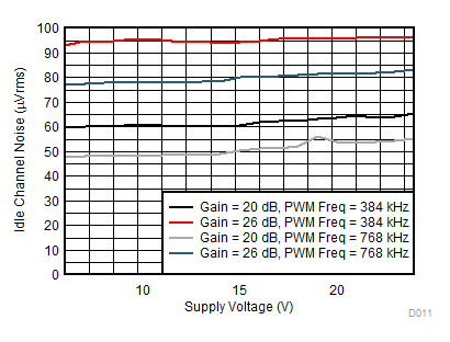
| ICN(SPK) | Idle channel noise | VPVDD = 12 V, SPK_GAIN = 20 dB, RSPK = 8 Ω, A-Weighted | 49 | µVRMS | ||
| VPVDD = 15 V, SPK_GAIN = 20 dB, RSPK = 8 Ω, A-Weighted | 59 | |||||
| VPVDD = 19 V, SPK_GAIN = 26 dB, RSPK = 8 Ω, A-Weighted | 81 | |||||
| VPVDD = 24 V, SPK_GAIN = 26 dB, RSPK = 8 Ω, A-Weighted | 82 | |||||
| PO(SPK) | Output Power (Per Channel) | VPVDD = 12 V, SPK_GAIN = 20 dB, RSPK = 4 Ω, THD+N = 0.1% | 14 | W | ||
| VPVDD = 12 V, SPK_GAIN = 20 dB, RSPK = 8 Ω, THD+N = 0.1% | 8 | |||||
| VPVDD = 15 V, SPK_GAIN = 26 dB, RSPK = 4 Ω, THD+N = 0.1% | 23 | |||||
| VPVDD = 15 V, SPK_GAIN = 26 dB, RSPK = 8 Ω, THD+N = 0.1% | 13 | |||||
| VPVDD = 19 V, SPK_GAIN = 26 dB, RSPK = 4 Ω, THD+N = 0.1% | 34 | |||||
| VPVDD = 19 V, SPK_GAIN = 26 dB, RSPK = 8 Ω, THD+N = 0.1% | 20 | |||||
| VPVDD = 24 V, SPK_GAIN = 26 dB, RSPK = 4 Ω, THD+N = 0.1% | 40 | |||||
| VPVDD = 24 V, SPK_GAIN = 26 dB, RSPK = 8 Ω, THD+N = 0.1% | 33 | |||||
| SNR | Signal-to-noise ratio (referenced to 0 dBFS input signal) | VPVDD = 12 V, SPK_GAIN = 20 dB, RSPK = 8 Ω, A-Weighted, –120 dBFS Input | 103 | dB | ||
| VPVDD = 15 V, SPK_GAIN = 26 dB, RSPK = 8 Ω, A-Weighted, –120 dBFS Input | 102 | |||||
| VPVDD = 19 V, SPK_GAIN = 26 dB, RSPK = 8 Ω, A-Weighted, –120 dBFS Input | 103 | |||||
| VPVDD = 24 V, SPK_GAIN = 26 dB, RSPK = 8 Ω, A-Weighted, –120 dBFS Input | 105 | |||||
| THD+NSPK | Total harmonic distortion and noise | VPVDD = 12 V, SPK_GAIN = 20 dB, RSPK = 4 Ω, PO = 1 W, f = 1kHz | 0.021% | |||
| VPVDD = 12 V, SPK_GAIN = 20 dB, RSPK = 8 Ω, PO = 1 W, f = 1kHz | 0.022% | |||||
| VPVDD = 15 V, SPK_GAIN = 26 dB, RSPK = 4 Ω, PO = 1 W, f = 1kHz | 0.02% | |||||
| VPVDD = 15 V, SPK_GAIN = 26 dB, RSPK = 8 Ω, PO = 1 W, f = 1kHz | 0.037% | |||||
| VPVDD = 19 V, SPK_GAIN = 26 dB, RSPK = 4 Ω, PO = 1 W, f = 1kHz | 0021% | |||||
| VPVDD = 19 V, SPK_GAIN = 26 dB, RSPK = 8 Ω, PO = 1 W, f = 1kHz | 0.028% | |||||
| VPVDD = 24 V, SPK_GAIN = 26 dB, RSPK = 4 Ω, PO = 1 W, f = 1kHz | 0.027% | |||||
| VPVDD = 24 V, SPK_GAIN = 26 dB, RSPK = 8 Ω, PO = 1 W, f = 1kHz | 0.038% | |||||
| X-talkSPK | Cross-talk (worst case between left-to-right and right-to-left coupling) | VPVDD = 12 V, SPK_GAIN = 20 dB, RSPK = 8 Ω, Input Signal 250 mVrms, 1-kHz Sine, across f(S) |
–90 | dB | ||
| VPVDD = 15 V, SPK_GAIN = 26 dBV, RSPK = 8 Ω, Input Signal 250 mVrms, 1-kHz Sine, across f(S) |
–102 | |||||
| VPVDD = 19 V, SPK_GAIN = 26 dBV, RSPK = 8 Ω, Input Signal 250 mVrms, 1-kHz Sine, across f(S) |
–93 | |||||
| VPVDD = 24 V, SPK_GAIN = 26 dBV, RSPK = 8 Ω, Input Signal 250 mVrms, 1-kHz Sine, across f(S) |
–93 | |||||
| SPEAKER AMPLIFIER (MONO PBTL) | ||||||
| |VOS| | Amplifier offset voltage | Measured differentially with zero input data, SPK_GAIN/FREQ pin configured for 20 dB gain, VPVDD = 12 V | 0.7 | mV | ||
| Measured differentially with zero input data, SPK_GAIN/FREQ pin configured for 26 dB gain, VPVDD = 24 V | 4 | |||||
| ICN | Idle channel noise | VPVDD = 12 V, SPK_GAIN = 20 dB, RSPK = 8 Ω, A-Weighted | 48 | µVRMS | ||
| VPVDD = 15 V, SPK_GAIN = 20 dB, RSPK = 8 Ω, A-Weighted | 49 | |||||
| VPVDD = 19 V, SPK_GAIN = 26 dB, RSPK = 8 Ω, A-Weighted | 83 | |||||
| VPVDD = 24 V, SPK_GAIN = 26 dB, RSPK = 8 Ω, A-Weighted | 82 | |||||
| PO | Output power (per channel) | VPVDD = 12 V, SPK_GAIN = 20 dB, RSPK = 2 Ω, THD+N = 0.1%, Unless otherwise noted | 30 | W | ||
| VPVDD = 12 V, SPK_GAIN = 20 dB, RSPK = 4 Ω, THD+N = 0.1%, Unless otherwise noted | 16 | |||||
| VPVDD = 12 V, SPK_GAIN = 20 dB, RSPK = 8 Ω, THD+N = 0.1% | 9 | |||||
| VPVDD = 15 V, SPK_GAIN = 26 dB, RSPK = 2 Ω, THD+N = 0.1%, Unless otherwise noted | 44 | |||||
| VPVDD = 15 V, SPK_GAIN = 26 dB, RSPK = 4 Ω, THD+N = 0.1%, Unless otherwise noted | 22 | |||||
| VPVDD = 15 V, SPK_GAIN = 26 dB, RSPK = 8 Ω, THD+N = 0.1% | 13 | |||||
| VPVDD = 19 V, SPK_GAIN = 26 dB, RSPK = 2 Ω, THD+N = 0.1%, Unless otherwise noted | 50 | |||||
| VPVDD = 19 V, SPK_GAIN = 26 dB, RSPK = 4 Ω, THD+N = 0.1%, Unless otherwise noted | 36 | |||||
| VPVDD = 19 V, SPK_GAIN = 26 dB, RSPK = 8 Ω, THD+N = 0.1% | 20 | |||||
| VPVDD = 24 V, SPK_GAIN = 26 dB, RSPK = 2 Ω, THD+N = 0.1%, Unless otherwise noted | 40 | |||||
| VPVDD = 24 V, SPK_GAIN = 26 dB, RSPK = 4 Ω, THD+N = 0.1%, Unless otherwise noted | 61 | |||||
| VPVDD = 24 V, SPK_GAIN = 26 dB, RSPK = 8 Ω, THD+N = 0.1% | 34 | |||||
| SNR | Signal-to-noise ratio (referenced to 0 dBFS input signal) |
VPVDD = 12 V, SPK_GAIN = 20 dB, RSPK = 8 Ω, A-Weighted, –120 dBFS Input | 105 | dB | ||
| VPVDD = 15 V, SPK_GAIN = 26 dB, RSPK = 8 Ω, A-Weighted, –120 dBFS Input | 104 | |||||
| VPVDD = 19 V, SPK_GAIN = 26 dB, RSPK = 8 Ω, A-Weighted, –120 dBFS Input | 105 | |||||
| VPVDD = 24 V, SPK_GAIN = 26 dB, RSPK = 8 Ω, A-Weighted, –120 dBFS Input | 107 | |||||
| THD+N | Total harmonic distortion and noise | VPVDD = 12 V, SPK_GAIN = 20 dB, RSPK = 2 Ω, PO = 1 W, f = 1kHz | 0.014% | |||
| VPVDD = 12 V, SPK_GAIN = 20 dB, RSPK = 4 Ω, PO = 1 W, f = 1kHz | 0.011% | |||||
| VPVDD = 12 V, SPK_GAIN = 20 dB, RSPK = 8 Ω, PO = 1 W, f = 1kHz | 0.014% | |||||
| VPVDD = 15 V, SPK_GAIN = 26 dB, RSPK = 2 Ω, PO = 1 W, f = 1kHz | 0.015% | |||||
| VPVDD = 15 V, SPK_GAIN = 26 dB, RSPK = 4 Ω, PO = 1 W, f = 1kHz | 0.013% | |||||
| VPVDD = 15 V, SPK_GAIN = 26 dB, RSPK = 8 Ω, PO = 1 W, f = 1kHz | 0.015% | |||||
| VPVDD = 19 V, SPK_GAIN = 26 dB, RSPK = 2 Ω, PO = 1 W, f = 1kHz | 0.018% | |||||
| V, RSPK = 4 Ω, PO = 1 W, f = 1kHz | 0.012% | |||||
| VPVDD = 19 V, SPK_GAIN = 26 dB, RSPK = 8 Ω, PO = 1 W, f = 1kHz | 0.020% | |||||
| VPVDD = 24 V, SPK_GAIN = 26 dB, RSPK = 2 Ω, PO = 1 W, f = 1kHz | 0.028% | |||||
| VPVDD = 24 V, SPK_GAIN = 26 dB, RSPK = 4 Ω, PO = 1 W, f = 1kHz | 0.02% | |||||
| VPVDD = 24 V, SPK_GAIN = 26 dB, RSPK = 8 Ω, PO = 1 W, f = 1kHz | 0.027% | |||||
7.6 Power Dissipation Characteristics
Free-air room temperature 25°C (unless otherwise noted)| VPVDD
(V) |
SPK_GAIN(1)(2)(3)
(dBV) |
fSPK_AMP
(kHz) |
STATE OF OPERATION |
RSPK
(Ω) |
IPVDD(4)
(mA) |
IDVDD(5)
(mA) |
PDISS
(W) |
|---|---|---|---|---|---|---|---|
| 7.4 | 20 | 384 | Idle | 4 | 21.30 | 59.70 | 0.355 |
| 6 | 21.33 | 59.68 | 0.355 | ||||
| 8 | 21.30 | 59.70 | 0.355 | ||||
| Mute | 4 | 21.33 | 58.82 | 0.352 | |||
| 6 | 21.34 | 58.81 | 0.352 | ||||
| 8 | 21.36 | 58.81 | 0.352 | ||||
| Standby | 4 | 2.08 | 12.41 | 0.056 | |||
| 6 | 2.11 | 12.41 | 0.057 | ||||
| 8 | 2.17 | 12.41 | 0.057 | ||||
| Powerdown | 4 | 2.03 | 0.730 | 0.017 | |||
| 6 | 2.04 | 0.740 | 0.018 | ||||
| 8 | 2.06 | 0.740 | 0.018 | ||||
| 768 | Idle | 4 | 27.48 | 59.7 | 0.400 | ||
| 6 | 27.49 | 59.73 | 0.401 | ||||
| 8 | 24.46 | 59.72 | 0.378 | ||||
| Mute | 4 | 27.50 | 58.8 | 0.398 | |||
| 6 | 27.51 | 58.8 | 0.398 | ||||
| 8 | 27.52 | 58.81 | 0.398 | ||||
| Standby | 4 | 2.04 | 12.41 | 0.056 | |||
| 6 | 2.08 | 12.41 | 0.056 | ||||
| 8 | 2.11 | 12.41 | 0.057 | ||||
| Powerdown | 4 | 2.06 | 0.73 | 0.018 | |||
| 6 | 2.07 | 0.74 | 0.018 | ||||
| 8 | 2.08 | 0.74 | 0.018 | ||||
| 11.1 | 20 | 384 | Idle | 4 | 24.33 | 59.74 | 0.467 |
| 6 | 24.32 | 59.74 | 0.467 | ||||
| 8 | 24.36 | 59.70 | 0.467 | ||||
| Mute | 4 | 24.36 | 58.81 | 0.464 | |||
| 6 | 24.32 | 58.82 | 0.464 | ||||
| 8 | 24.37 | 58.84 | 0.465 | ||||
| Standby | 4 | 3.58 | 12.40 | 0.081 | |||
| 6 | 3.57 | 12.41 | 0.081 | ||||
| 8 | 3.58 | 12.42 | 0.081 | ||||
| Powerdown | 4 | 3.52 | 0.74 | 0.042 | |||
| 6 | 3.52 | 0.74 | 0.042 | ||||
| 8 | 3.54 | 0.74 | 0.042 | ||||
| 768 | Idle | 4 | 30.70 | 59.70 | 0.538 | ||
| 6 | 30.65 | 59.72 | 0.537 | ||||
| 8 | 30.67 | 59.71 | 0.537 | ||||
| Mute | 4 | 3.072 | 58.80 | 0.528 | |||
| 6 | 30.69 | 58.81 | 0.535 | ||||
| 8 | 30.69 | 58.81 | 0.535 | ||||
| Standby | 4 | 3.54 | 12.40 | 0.080 | |||
| 6 | 3.54 | 12.41 | 0.080 | ||||
| 8 | 3.58 | 12.42 | 0.081 | ||||
| Powerdown | 4 | 3.53 | 0.74 | 0.042 | |||
| 6 | 3.53 | 0.74 | 0.042 | ||||
| 8 | 3.55 | 0.74 | 0.042 | ||||
| 12 | 20 | 384 | Idle | 4 | 25.07 | 59.72 | 0.498 |
| 6 | 25.08 | 59.73 | 0.498 | ||||
| 8 | 25.10 | 59.71 | 0.498 | ||||
| Mute | 4 | 25.12 | 58.84 | 0.496 | |||
| 6 | 25.08 | 58.82 | 0.495 | ||||
| 8 | 25.11 | 58.82 | 0.495 | ||||
| Standby | 4 | 3.92 | 12.40 | 0.088 | |||
| 6 | 3.93 | 12.41 | 0.088 | ||||
| 8 | 3.94 | 12.41 | 0.088 | ||||
| Powerdown | 4 | 3.87 | 0.75 | 0.049 | |||
| 6 | 3.85 | 0.74 | 0.049 | ||||
| 8 | 3.87 | 0.75 | 0.049 | ||||
| 768 | Idle | 4 | 31.31 | 59.72 | 0.573 | ||
| 6 | 31.29 | 59.71 | 0.573 | ||||
| 8 | 31.31 | 59.74 | 0.573 | ||||
| Mute | 4 | 31.31 | 58.80 | 0.570 | |||
| 6 | 31.33 | 58.81 | 0.570 | ||||
| 8 | 31.32 | 58.81 | 0.570 | ||||
| Standby | 4 | 3.88 | 12.40 | 0.087 | |||
| 6 | 3.90 | 12.41 | 0.088 | ||||
| 8 | 3.91 | 12.41 | 0.088 | ||||
| Powerdown | 4 | 3.89 | 0.75 | 0.049 | |||
| 6 | 3.91 | 0.74 | 0.049 | ||||
| 8 | 3.88 | 0.75 | 0.049 | ||||
| 15 | 26 | 384 | Idle | 4 | 27.94 | 59.73 | 0.616 |
| 6 | 27.91 | 59.75 | 0.616 | ||||
| 8 | 27.75 | 59.69 | 0.613 | ||||
| Mute | 4 | 27.98 | 58.84 | 0.614 | |||
| 6 | 27.94 | 58.87 | 0.613 | ||||
| 8 | 27.88 | 58.85 | 0.612 | ||||
| Standby | 4 | 5.09 | 12.41 | 0.117 | |||
| 6 | 5.12 | 12.41 | 0.118 | ||||
| 8 | 5.19 | 12.41 | 0.119 | ||||
| Powerdown | 4 | 5.02 | 0.74 | 0.078 | |||
| 6 | 5.06 | 0.74 | 0.078 | ||||
| 8 | 5.14 | 0.74 | 0.080 | ||||
| 768 | Idle | 4 | 33.05 | 59.7 | 0.693 | ||
| 6 | 33.03 | 59.72 | 0.693 | ||||
| 8 | 33.08 | 59.68 | 0.693 | ||||
| Mute | 4 | 33.03 | 58.81 | 0.690 | |||
| 6 | 33.04 | 58.81 | 0.690 | ||||
| 8 | 33.05 | 58.80 | 0.690 | ||||
| Standby | 4 | 5.07 | 12.41 | 0.117 | |||
| 6 | 5.09 | 12.41 | 0.117 | ||||
| 8 | 5.14 | 12.41 | 0.118 | ||||
| Powerdown | 4 | 5.02 | 0.74 | 0.078 | |||
| 6 | 5.04 | 0.74 | 0.078 | ||||
| 8 | 5.09 | 0.74 | 0.079 | ||||
| 19.6 | 26 | 384 | Idle | 4 | 32.27 | 59.77 | 0.830 |
| 6 | 32.19 | 59.76 | 0.828 | ||||
| 8 | 32.08 | 59.75 | 0.826 | ||||
| Mute | 4 | 32.27 | 58.85 | 0.827 | |||
| 6 | 32.24 | 58.87 | 0.826 | ||||
| 8 | 32.22 | 58.86 | 0.826 | ||||
| Standby | 4 | 6.95 | 12.40 | 0.177 | |||
| 6 | 6.93 | 12.42 | 0.177 | ||||
| 8 | 7.00 | 12.41 | 0.178 | ||||
| Powerdown | 4 | 6.89 | 0.74 | 0.137 | |||
| 6 | 6.90 | 0.74 | 0.138 | ||||
| 8 | 6.96 | 0.73 | 0.139 | ||||
| 768 | Idle | 4 | 34.99 | 59.74 | 0.883 | ||
| 6 | 34.95 | 59.74 | 0.882 | ||||
| 8 | 34.97 | 59.71 | 0.882 | ||||
| Mute | 4 | 34.96 | 58.85 | 0.879 | |||
| 6 | 34.98 | 58.83 | 0.880 | ||||
| 8 | 34.96 | 58.81 | 0.879 | ||||
| Standby | 4 | 6.93 | 12.40 | 0.177 | |||
| 6 | 6.93 | 12.42 | 0.177 | ||||
| 8 | 6.98 | 12.41 | 0.178 | ||||
| Powerdown | 4 | 6.84 | 0.74 | 0.137 | |||
| 6 | 6.89 | 0.74 | 0.137 | ||||
| 8 | 6.90 | 0.73 | 0.138 | ||||
| 24 | 26 | 384 | Idle | 4 | 36.93 | 59.80 | 1.084 |
| 6 | 36.87 | 59.81 | 1.082 | ||||
| 8 | 36.77 | 59.76 | 1.080 | ||||
| Mute | 4 | 36.94 | 58.91 | 1.081 | |||
| 6 | 36.89 | 58.89 | 1.080 | ||||
| 8 | 36.85 | 58.90 | 1.079 | ||||
| Standby | 4 | 8.73 | 12.40 | 0.250 | |||
| 6 | 8.72 | 12.40 | 0.250 | ||||
| 8 | 8.71 | 12.40 | 0.250 | ||||
| Powerdown | 4 | 8.64 | 0.74 | 0.210 | |||
| 6 | 8.66 | 0.74 | 0.210 | ||||
| 8 | 8.69 | 0.73 | 0.211 | ||||
| 768 | Idle | 4 | 36.84 | 59.73 | 1.081 | ||
| 6 | 36.86 | 59.76 | 1.082 | ||||
| 8 | 36.83 | 59.78 | 1.081 | ||||
| Mute | 4 | 36.85 | 58.85 | 1.079 | |||
| 6 | 36.84 | 58.84 | 1.078 | ||||
| 8 | 36.82 | 58.83 | 1.078 | ||||
| Standby | 4 | 8.66 | 12.40 | 0.249 | |||
| 6 | 8.68 | 12.40 | 0.249 | ||||
| 8 | 8.71 | 12.40 | 0.250 | ||||
| Powerdown | 4 | 8.63 | 0.74 | 0.210 | |||
| 6 | 8.64 | 0.74 | 0.210 | ||||
| 8 | 8.65 | 0.73 | 0.210 |
7.7 MCLK Timing
See Figure 18.| MIN | NOM | MAX | UNIT | ||
|---|---|---|---|---|---|
| tMCLK | MCLK period | 20 | 1000 | ns | |
| tMCLKH | MCLK pulse width, high | 9 | ns | ||
| tMCLKL | MCLK pulse width, low | 9 | ns | ||
7.8 Serial Audio Port Timing – Slave Mode
See Figure 19.| MIN | NOM | MAX | UNIT | ||
|---|---|---|---|---|---|
| fSCLK | SCLK frequency | 1.024 | MHz | ||
| tSCLK | SCLK period | 40 | ns | ||
| tSCLKL | SCLK pulse width, low | 16 | ns | ||
| tSCLKH | SCLK pulse width, high | 16 | ns | ||
| tSL | SCLK rising to LRCK/FS edge | 8 | ns | ||
| tLS | LRCK/FS Edge to SCLK rising edge | 8 | ns | ||
| tSU | Data setup time, before SCLK rising edge | 8 | ns | ||
| tDH | Data hold time, after SCLK rising edge | 8 | ns | ||
| tDFS | Data delay time from SCLK falling edge | 15 | ns | ||
7.9 Serial Audio Port Timing – Master Mode
See Figure 20.| MIN | NOM | MAX | UNIT | ||
|---|---|---|---|---|---|
| tSCLK | SCLK period | 40 | ns | ||
| tSCLKL | SCLK pulse width, low | 16 | ns | ||
| tSCLKH | SCLK pulse width, high | 16 | ns | ||
| tLRD | LRCK/FS delay time from to SCLK falling edge | –10 | 20 | ns | |
| tSU | Data setup time, before SCLK rising edge | 8 | ns | ||
| tDH | Data hold time, after SCLK rising edge | 8 | ns | ||
| tDFS | Data delay time from SCLK falling edge | 15 | ns | ||
7.10 I2C Bus Timing – Standard
| MIN | MAX | UNIT | ||
|---|---|---|---|---|
| fSCL | SCL clock frequency | 100 | kHz | |
| tBUF | Bus free time between a STOP and START condition | 4.7 | µs | |
| tLOW | Low period of the SCL clock | 4.7 | µs | |
| tHI | High period of the SCL clock | 4 | µs | |
| tRS-SU | Setup time for (repeated) START condition | 4.7 | µs | |
| tS-HD | Hold time for (repeated) START condition | 4 | µs | |
| tD-SU | Data setup time | 250 | ns | |
| tD-HD | Data hold time | 0 | 900 | ns |
| tSCL-R | Rise time of SCL signal | 20 + 0.1CB | 1000 | ns |
| tSCL-R1 | Rise time of SCL signal after a repeated START condition and after an acknowledge bit | 20 + 0.1CB | 1000 | ns |
| tSCL-F | Fall time of SCL signal | 20 + 0.1CB | 1000 | ns |
| tSDA-R | Rise time of SDA signal | 20 + 0.1CB | 1000 | ns |
| tSDA-F | Fall time of SDA signal | 20 + 0.1CB | 1000 | ns |
| tP-SU | Setup time for STOP condition | 4 | µs | |
7.11 I2C Bus Timing – Fast
See Figure 21.| MIN | MAX | UNIT | ||
|---|---|---|---|---|
| fSCL | SCL clock frequency | 400 | kHz | |
| tBUF | Bus free time between a STOP and START condition | 1.3 | µs | |
| tLOW | Low period of the SCL clock | 1.3 | µs | |
| tHI | High period of the SCL clock | 600 | ns | |
| tRS-SU | Setup time for (repeated)START condition | 600 | ns | |
| tRS-HD | Hold time for (repeated)START condition | 600 | ns | |
| tD-SU | Data setup time | 100 | ns | |
| tD-HD | Data hold time | 0 | 900 | ns |
| tSCL-R | Rise time of SCL signal | 20 + 0.1CB | 300 | ns |
| tSCL-R1 | Rise time of SCL signal after a repeated START condition and after an acknowledge bit | 20 + 0.1CB | 300 | ns |
| tSCL-F | Fall time of SCL signal | 20 + 0.1CB | 300 | ns |
| tSDA-R | Rise time of SDA signal | 20 + 0.1CB | 300 | ns |
| tSDA-F | Fall time of SDA signal | 20 + 0.1CB | 300 | ns |
| tP-SU | Setup time for STOP condition | 600 | ns | |
| tSP | Pulse width of spike suppressed | 50 | ns | |
 Figure 18. Timing Requirements for MCLK Input
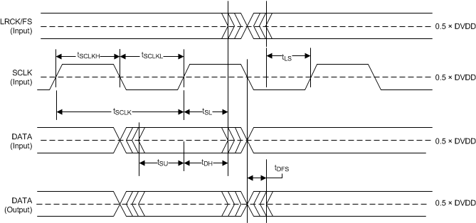 Figure 19. Serial Audio Port Timing in Slave Mode
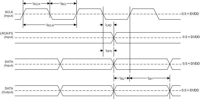 Figure 20. Serial Audio Port Timing in Master Mode
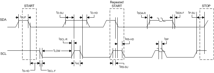 Figure 21. I2C Communication Port Timing Diagram
 Figure 22. SPK_MUTE Timing Diagram for Soft Mute Operation via Hardware Pin
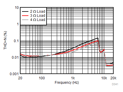
7.13 Typical Characteristics
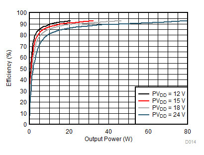
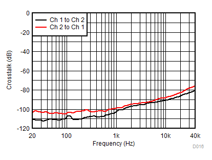
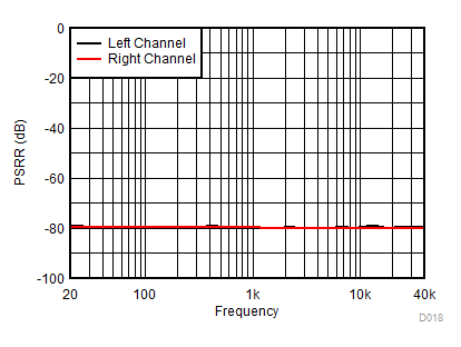
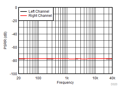
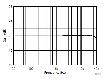
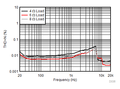
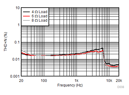
All performance plots were taken using the TAS5782MEVM Board at room temperature, unless otherwise noted. The term "traditional LC filter" refers to the output filter that is present by default on the TAS5782MEVM Board.
Table 1. Quick Reference Table
| OUTPUT CONFIGURATIONS |
PLOT TITLE | FIGURE NUMBER |
|---|---|---|
| Bridge Tied Load (BTL) Configuration Curves | Frequency Response | Figure 42 |
| Output Power vs PVDD | Figure 23 | |
| THD+N vs Frequency, VPVDD = 12 V | Figure 24 | |
| THD+N vs Frequency, VPVDD = 15 V | Figure 25 | |
| THD+N vs Frequency, VPVDD = 18 V | Figure 26 | |
| THD+N vs Frequency, VPVDD = 24 V | Figure 27 | |
| THD+N vs Power, VPVDD = 12 V | Figure 28 | |
| THD+N vs Power, VPVDD = 15 V | Figure 29 | |
| THD+N vs Power, VPVDD = 18 V | Figure 30 | |
| THD+N vs Power, VPVDD = 24 V | Figure 31 | |
| Idle Channel Noise vs PVDD | Figure 32 | |
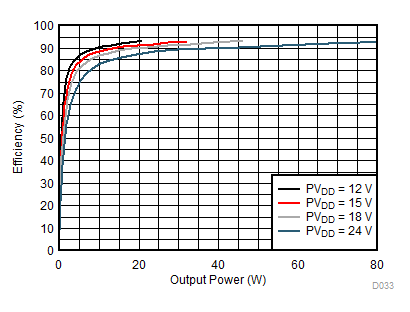
| Efficiency vs Output Power | Figure 33 | |
| Efficiency vs Output Power | Figure 34 | |
| Efficiency vs Output Power | Figure 35 | |
| Idle Current Draw (Filterless) vs PVDD | Figure 36 | |
| Crosstalk vs. Frequency | Figure 37 | |
| PVDD PSRR vs Frequency | Figure 38 | |
| DVDD PSRR vs Frequency | Figure 39 | |
| AVDD PSRR vs Frequency | Figure 40 | |
| CPVDD PSRR vs Frequency | Figure 41 | |
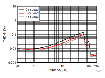
| THD+N vs Frequency, VPVDD = 12 V | Figure 43 | |
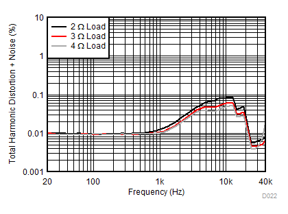
| THD+N vs Frequency, VPVDD = 15 V | Figure 44 | |
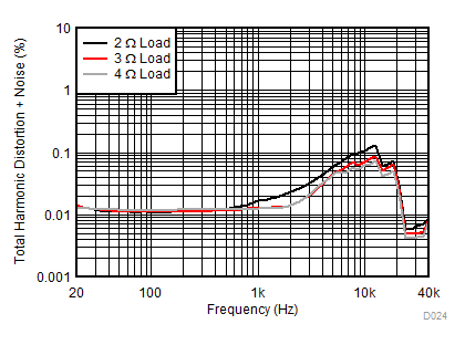
| THD+N vs Frequency, VPVDD = 18 V | Figure 45 | |
| THD+N vs Frequency, VPVDD = 24 V | Figure 46 | |
| Parallel Bridge Tied Load (PBTL) Configuration | Output Power vs PVDD | Figure 47 |
| THD+N vs Frequency, VPVDD = 12 V | Figure 48 | |
| THD+N vs Frequency, VPVDD = 15 V | Figure 49 | |
| THD+N vs Frequency, VPVDD = 18 V | Figure 50 | |
| THD+N vs Frequency, VPVDD = 24 V | Figure 51 | |
| THD+N vs Power, VPVDD = 12 V | Figure 52 | |
| THD+N vs Power, VPVDD = 15 V | Figure 53 | |
| THD+N vs Power, VPVDD = 18 V | Figure 54 | |
| THD+N vs Power, VPVDD = 24 V | Figure 55 | |
| Idle Channel Noise vs PVDD | Figure 56 | |
| Efficiency vs Output Power | Figure 57 | |
| THD+N vs Frequency, VPVDD = 12 V | Figure 60 | |
| THD+N vs Frequency, VPVDD = 15 V | Figure 61 | |
| THD+N vs Frequency, VPVDD = 18 V | Figure 62 | |
| THD+N vs Frequency, VPVDD = 24 V | Figure 63 |
7.13.1 Bridge Tied Load (BTL) Configuration Curves
Free-air room temperature 25°C (unless otherwise noted) Measurements were made using TAS5782MEVM board and Audio Precision System 2722 with Analog Analyzer filter set to 40-kHz brickwall filter. All measurements taken with audio frequency set to 1 kHz and device PWM frequency set to 768 kHz, unless otherwise noted. For both the BTL plots and the PBTL plots, the LC filter used was 4.7 µH / 0.68 µF. Return to Quick Reference Table.

| AV(SPK_AMP) = 26 dBV |

| AV(SPK_AMP) = 20 dBV | PO = 1 W | VPVDD = 15 V |
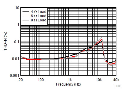
| AV(SPK_AMP) = 20 dBV | PO = 1 W | VPVDD = 12 V |
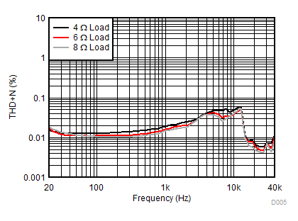
| AV(SPK_AMP) = 26 dBV | PO = 1 W | VPVDD = 18 V |

| AV(SPK_AMP) = 26 dBV | PO = 1 W | VPVDD = 24 V |
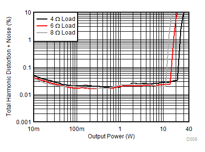
| AV(SPK_AMP) = 20 dBV | VPVDD = 15 V |
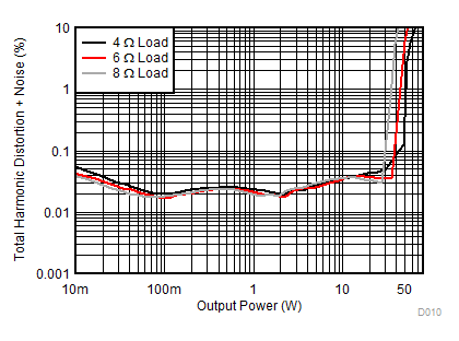
| AV(SPK_AMP) = 26 dBV | VPVDD = 24 V |
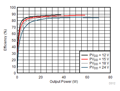
| RSPK = 4 Ω |
| RSPK = 8 Ω |
| AV(SPK_AMP) = 26 dBV | VPVDD = 24 V |
| AV(SPK_AMP) = 26 dBV | VPVDD = 24 V |
| VDVDD = 3.3 V + 250 mVac |
| AV(SPK_AMP) = 26 dBV | VPVDD = 24 V |
| VCPVDD = 3.3 V + 250 mVac |

| AV(SPK_AMP) = 20 dB | POUT = 1 W | PVDD = 12 V |
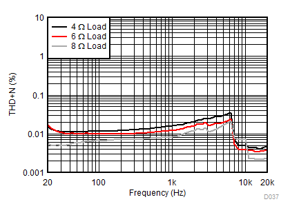
| AV(SPK_AMP) = 20 dB | POUT = 1 W | PVDD = 18 V |
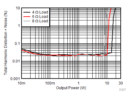
| AV(SPK_AMP) = 20 dBV | VPVDD = 12 V |
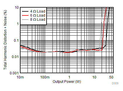
| AV(SPK_AMP) = 26 dBV | VPVDD = 18 V |
| RSPK = 4 Ω |
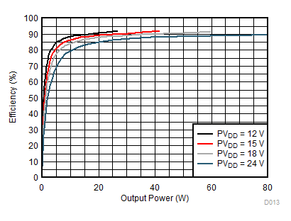
| RSPK = 6 Ω |
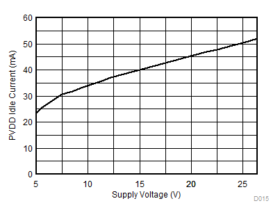
| fSPK_AMP = 768 kHz | RSPK = 8 Ω |
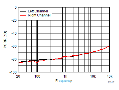
| AV(SPK_AMP) = 26 dBV | VPVDD = 24 V + 250 mVac |
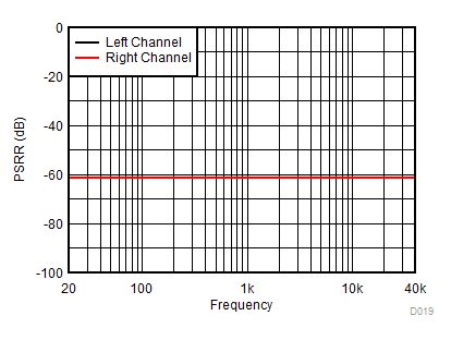
| AV(SPK_AMP) = 26 dBV | VPVDD = 24 V |
| VAVDD = 3.3 V + 250 mVac |
| AV(SPK_AMP) = 20 dB | POUT = 1 W | PVDD = 12 V |
| AV(SPK_AMP) = 20 dB | POUT = 1 W | PVDD = 15 V |
| AV(SPK_AMP) = 20 dB | POUT = 1 W | PVDD = 24 V |
7.13.2 Parallel Bridge Tied Load (PBTL) Configuration
Return to Quick Reference Table.
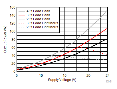
| AV(SPK_AMP) = 26 dBV | ||
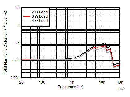
| AV(SPK_AMP) = 20 dBV | PO = 1 W | VPVDD = 15 V |
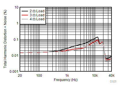
| AV(SPK_AMP) = 26 dBV | PO = 1 W | VPVDD = 24 V |
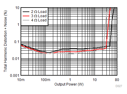
| AV(SPK_AMP) = 20 dBV
|
VPVDD = 15 V |
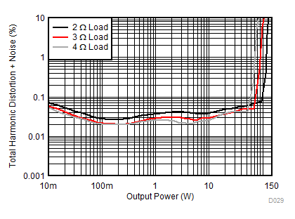
| AV(SPK_AMP) = 20 dBV
|
VPVDD = 24 V |

| AV(SPK_AMP) = 26 dBV | RSPK = 2 Ω |
| AV(SPK_AMP) = 20 dBV | RSPK = 4 Ω |
| AV(SPK_AMP) = 20 dB | POUT = 1 W | PVDD = 15 V |

| AV(SPK_AMP) = 20 dB | POUT = 1 W | PVDD = 24 V |
| AV(SPK_AMP) = 20 dBV | PO = 1 W | VPVDD = 12 V |
| AV(SPK_AMP) = 26 dBV | PO = 1 W | VPVDD = 18 V |
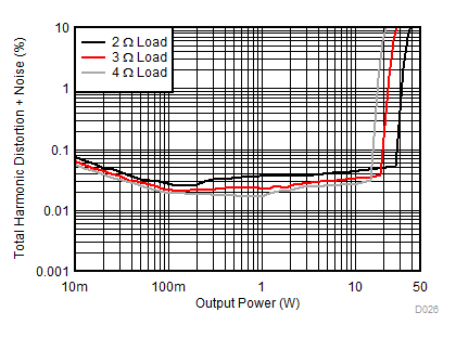
| AV(SPK_AMP) = 20 dBV | VPVDD = 12 V |
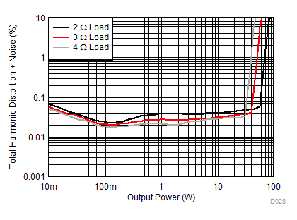
| AV(SPK_AMP) = 26 dBV
|
VPVDD = 18 V |
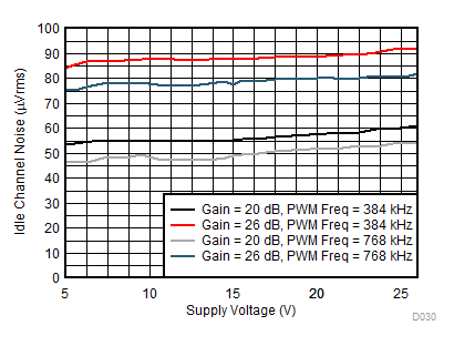
| RSPK = 4 Ω |
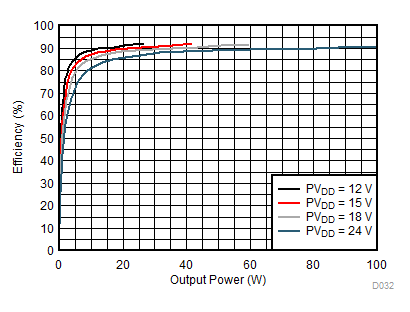
| AV(SPK_AMP) = 20 dBV | RSPK = 3 Ω |

| AV(SPK_AMP) = 20 dB | POUT = 1 W | PVDD = 12 V |
| AV(SPK_AMP) = 20 dB | POUT = 1 W | PVDD = 18 V |