SCPS234A September 2016 – February 2023 TCA6408A-Q1
PRODUCTION DATA
- 1 Features
- 2 Applications
- 3 Description
- 4 Revision History
- 5 Pin Configuration and Functions
- 6 Specifications
- 7 Parameter Measurement Information
- 8 Detailed Description
- 9 Application and Implementation
- 10Device and Documentation Support
- 11Support Resources
- 12Mechanical, Packaging, and Orderable Information
Package Options
Mechanical Data (Package|Pins)
- PW|16
Thermal pad, mechanical data (Package|Pins)
Orderable Information
7 Parameter Measurement Information

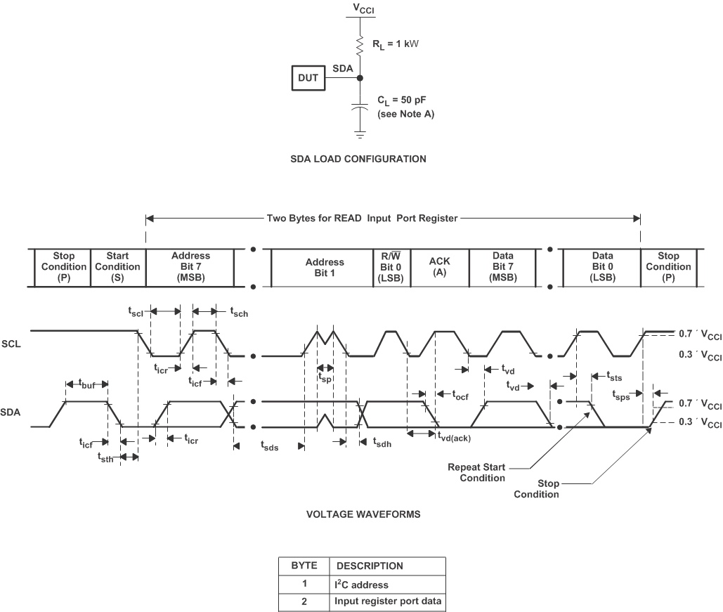
A. CL includes probe and jig capacitance. tocf is measured with CL of 10 pF or 400 pF.
B. All inputs are supplied by generators having the following characteristics: PRR ≤ 10 MHz, ZO = 50 Ω, tr/tf ≤ 30 ns.
Figure 7-1 I2C Interface Load Circuit and Voltage WaveformsA. CL includes probe and jig capacitance.
B. All inputs are supplied by generators having the following characteristics: PRR ≤ 10 MHz, ZO = 50 Ω, tr/tf ≤ 30 ns.
Figure 7-2 Interrupt Load Circuit and Voltage WaveformsA. CL includes probe and jig capacitance.
B. tpv is measured from 0.7 × VCC on SCL to 50% I/O (Pn) output.
C. All inputs are supplied by generators having the following characteristics: PRR ≤ 10 MHz, ZO = 50 Ω, tr/tf ≤ 30 ns.
D. The outputs are measured one at a time, with one transition per measurement.
Figure 7-3 P-Port Load Circuit and Timing Waveforms
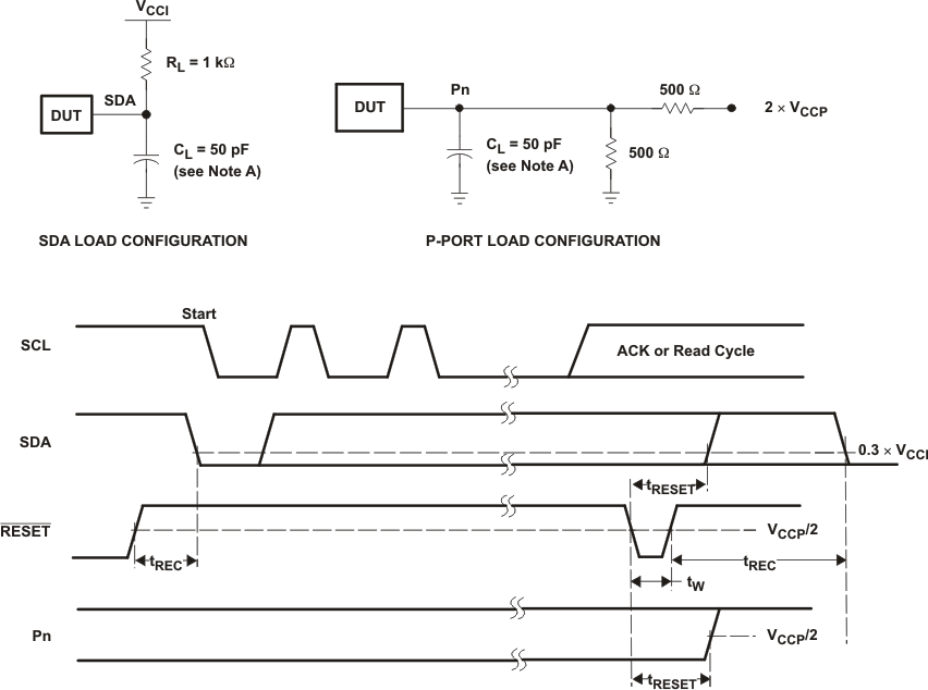
A. CL includes probe and jig capacitance.
B. All inputs are supplied by generators having the following characteristics: PRR ≤ 10 MHz, ZO = 50 Ω, tr/tf ≤ 30 ns.
C. The outputs are measured one at a time, with one transition per measurement.
D. I/Os are configured as inputs.
Figure 7-4 Reset Load Circuits and Voltage Waveforms