SCPS234A September 2016 – February 2023 TCA6408A-Q1
PRODUCTION DATA
- 1 Features
- 2 Applications
- 3 Description
- 4 Revision History
- 5 Pin Configuration and Functions
- 6 Specifications
- 7 Parameter Measurement Information
- 8 Detailed Description
- 9 Application and Implementation
- 10Device and Documentation Support
- 11Support Resources
- 12Mechanical, Packaging, and Orderable Information
Package Options
Mechanical Data (Package|Pins)
- PW|16
Thermal pad, mechanical data (Package|Pins)
Orderable Information
8.5.1 I2C Interface
The TCA6408A-Q1 has a standard bidirectional I2C interface that is controlled by a controller device in order to be configured or read the status of this device. Each target on the I2C bus has a specific device address to differentiate between other target devices that are on the same I2C bus. Many target devices require configuration upon startup to set the behavior of the device. This is typically done when the controller accesses internal register maps of the target, which have unique register addresses. A device can have one or multiple registers where data is stored, written, or read.
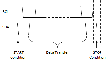
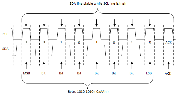
The physical I2C interface consists of the serial clock (SCL) and serial data (SDA) lines. Both SDA and SCL lines must be connected to VCC through a pull-up resistor. The size of the pull-up resistor is determined by the amount of capacitance on the I2C lines. (For further details, see the application report, I2C Pull-up Resistor Calculation (SLVA689)). Data transfer may be initiated only when the bus is idle. A bus is considered idle if both SDA and SCL lines are high after a STOP condition. See Figure 8-3 and Figure 8-4.
The following is the general procedure for a controller to access a target device:
- If a controller wants to send data to a target:
- Controller-transmitter sends a START condition and addresses the target-receiver.
- Controller-transmitter sends data to target-receiver.
- Controller-transmitter terminates the transfer with a STOP condition.
- If a controller wants to receive or read data from a target:
- Controller-receiver sends a START condition and addresses the target-transmitter.
- Controller-receiver sends the requested register to read to target-transmitter.
- Controller-receiver receives data from the target-transmitter.
- Controller-receiver terminates the transfer with a STOP condition.
 Figure 8-3 Definition of Start and Stop Conditions
 Figure 8-4 Bit Transfer
Table 8-2 shows the interface definition for the TCA6408A-Q1 device.
| BYTE | BIT | |||||||
|---|---|---|---|---|---|---|---|---|
| 7 (MSB) | 6 | 5 | 4 | 3 | 2 | 1 | 0 (LSB) | |
| I2C target address | L | H | L | L | L | L | ADDR | R/ W |
| I/O data bus | P7 | P6 | P5 | P4 | P3 | P2 | P1 | P0 |