SCPS193D July 2010 – January 2023 TCA6424A
PRODUCTION DATA
- 1 Features
- 2 Description
- 3 Revision History
- 4 Description (continued)
- 5 Pin Configuration and Functions
- 6 Specifications
- 7 Parameter Measurement Information
- 8 Detailed Description
- 9 Application and Implementation
- 10Device and Documentation Support
Package Options
Mechanical Data (Package|Pins)
- RGJ|32
Thermal pad, mechanical data (Package|Pins)
Orderable Information
5 Pin Configuration and Functions

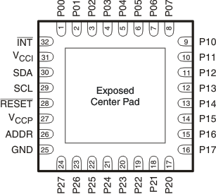
If used, the exposed center pad must be connected as a secondary ground or left electrically open.
Figure 5-1 RGJ Package(Bottom View)
Table 5-1 Pin Functions
| PIN | DESCRIPTION | |
|---|---|---|
| PIN NO. | NAME | |
| 1 | P00 | P-port input/output (push-pull design structure). At power on, P00 is configured as an input. |
| 2 | P01 | P-port input/output (push-pull design structure). At power on, P01 is configured as an input. |
| 3 | P02 | P-port input/output (push-pull design structure). At power on, P02 is configured as an input. |
| 4 | P03 | P-port input/output (push-pull design structure). At power on, P03 is configured as an input. |
| 5 | P04 | P-port input/output (push-pull design structure). At power on, P04 is configured as an input. |
| 6 | P05 | P-port input/output (push-pull design structure). At power on, P05 is configured as an input. |
| 7 | P06 | P-port input/output (push-pull design structure). At power on, P06 is configured as an input. |
| 8 | P07 | P-port input/output (push-pull design structure). At power on, P07 is configured as an input. |
| 9 | P10 | P-port input/output (push-pull design structure). At power on, P10 is configured as an input. |
| 10 | P11 | P-port input/output (push-pull design structure). At power on, P11 is configured as an input. |
| 11 | P12 | P-port input/output (push-pull design structure). At power on, P12 is configured as an input. |
| 12 | P13 | P-port input/output (push-pull design structure). At power on, P13 is configured as an input. |
| 13 | P14 | P-port input/output (push-pull design structure). At power on, P14 is configured as an input. |
| 14 | P15 | P-port input/output (push-pull design structure). At power on, P15 is configured as an input. |
| 15 | P16 | P-port input/output (push-pull design structure). At power on, P16 is configured as an input. |
| 16 | P17 | P-port input/output (push-pull design structure). At power on, P17 is configured as an input. |
| 17 | P20 | P-port input/output (push-pull design structure). At power on, P20 is configured as an input. |
| 18 | P21 | P-port input/output (push-pull design structure). At power on, P21 is configured as an input. |
| 19 | P22 | P-port input/output (push-pull design structure). At power on, P22 is configured as an input. |
| 20 | P23 | P-port input/output (push-pull design structure). At power on, P23 is configured as an input. |
| 21 | P24 | P-port input/output (push-pull design structure). At power on, P24 is configured as an input. |
| 22 | P25 | P-port input/output (push-pull design structure). At power on, P25 is configured as an input. |
| 23 | P26 | P-port input/output (push-pull design structure). At power on, P26 is configured as an input. |
| 24 | P27 | P-port input/output (push-pull design structure). At power on, P27 is configured as an input. |
| 25 | GND | Ground |
| 26 | ADDR | Address input. Connect directly to VCCP or ground. |
| 27 | VCCP | Supply voltage of TCA6424A for P port |
| 28 | RESET | Active-low reset input. Connect to VCCI through a pullup resistor, if no active connection is used. |
| 29 | SCL | Serial clock bus. Connect to VCCI through a pullup resistor. |
| 30 | SDA | Serial data bus. Connect to VCCI through a pullup resistor. |
| 31 | VCCI | Supply voltage of I2C bus. Connect directly to the VCC of the external I2C controller. Provides voltage-level translation. |
| 32 | INT | Interrupt output. Connect to VCCI through a pullup resistor. |