SCPS272C October 2019 – January 2021 TCA9511A
PRODUCTION DATA
- 1 Features
- 2 Applications
- 3 Description
- 4 Revision History
- 5 Pin Configuration and Functions
- 6 Specifications
- 7 Parameter Measurement Information
- 8 Detailed Description
- 9 Application Information Disclaimer
- 10Power Supply Recommendations
- 11Layout
- 12Device and Documentation Support
- 13Mechanical, Packaging, and Orderable Information
Package Options
Mechanical Data (Package|Pins)
- DGK|8
Thermal pad, mechanical data (Package|Pins)
- DGK|8
Orderable Information
5 Pin Configuration and Functions
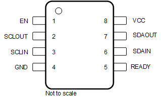
 Figure 5-1 8-Pin VSSOP, DGK Package (Top
View)
Figure 5-1 8-Pin VSSOP, DGK Package (Top
View)Table 5-1 Pin Functions
| PIN | I/O | DESCRIPTION | |
|---|---|---|---|
| NAME | NO. | ||
| EN | 1 | I | Active-high chip enable pin. If EN is low, the TCA9511A is in a low current mode. It also disables the rise-time accelerators, disables the bus pre-charge circuitry, drives READY low, isolates SDAIN from SDAOUT and isolates SCLIN from SCLOUT. EN should be high (at VCC) for normal operation. Connect EN to VCC if this feature is not being used. |
| SCLOUT | 2 | I/O | Serial clock output. Connect this pin to the SCL bus on the card. |
| SCLIN | 3 | I/O | Serial clock input. Connect this pin to the SCL bus on the backplane. |
| GND | 4 | - | Supply ground |
| READY | 5 | O | Connection flag/rise-time accelerator control. Ready is low when either EN is low or the start-up sequence has not been completed. READY goes high when EN is high and start-up is complete. Connect a 10-kΩ resistor from this pin to VCC to provide the pull-up current. |
| SDAIN | 6 | I/O | Serial data input. Connect this pin to the SDA bus on the backplane. |
| SDAOUT | 7 | I/O | Serial data output. Connect this pin to the SDA bus on the card. |
| VCC | 8 | - | Supply Power. Main input power supply from backplane. This is the supply voltage for the devices on the backplane I2C buses. Connect pull-up resistors from SDAIN and SCLIN (and also from SDAOUT and SCLOUT) to this supply. It is recommended to place a bypass capacitor of 0.1 μF close to this pin for best results. |