SCPS272C October   2019  – January 2021 TCA9511A

PRODUCTION DATA  

  1. Features
  2. Applications
  3. Description
  4. Revision History
  5. Pin Configuration and Functions
  6. Specifications
    1. 6.1 Absolute Maximum Ratings
    2. 6.2 ESD Ratings
    3. 6.3 Recommended Operating Conditions
    4. 6.4 Thermal Information
    5. 6.5 Electrical Characteristics
    6. 6.6 Timing Requirements
    7. 6.7 Switching Characteristics
    8. 6.8 Typical Characteristics
  7. Parameter Measurement Information
  8. Detailed Description
    1. 8.1 Overview
    2. 8.2 Functional Block Diagram
    3. 8.3 Feature Description
      1. 8.3.1 Hot bus insertion
      2. 8.3.2 Pre-charge voltage
      3. 8.3.3 Rise time accelerators
      4. 8.3.4 Bus ready output indicator
      5. 8.3.5 Powered-off high impedance for I2C and I/O pins
      6. 8.3.6 Supports clock stretching and arbitration
    4. 8.4 Device Functional Modes
      1. 8.4.1 Start-up and precharge
      2. 8.4.2 Bus idle
      3. 8.4.3 Bus active
  9. Application Information Disclaimer
    1. 9.1 Application Information
    2. 9.2 Typical Application
      1. 9.2.1 Design Requirements
        1. 9.2.1.1 Series connections
        2. 9.2.1.2 Multiple connections to a common node
        3. 9.2.1.3 Propagation delays
      2. 9.2.2 Detailed Design Procedure
      3. 9.2.3 Application Curves
    3. 9.3 Typical Application on a Backplane
      1. 9.3.1 Design Requirements
      2. 9.3.2 Detailed Design Procedure
  10. 10Power Supply Recommendations
    1. 10.1 Power Supply Best Practices
    2. 10.2 Power-on Reset Requirements
  11. 11Layout
    1. 11.1 Layout Guidelines
    2. 11.2 Layout Example
  12. 12Device and Documentation Support
    1. 12.1 Receiving Notification of Documentation Updates
    2. 12.2 Support Resources
    3. 12.3 Trademarks
    4. 12.4 Electrostatic Discharge Caution
    5. 12.5 Glossary
  13. 13Mechanical, Packaging, and Orderable Information

Package Options

Mechanical Data (Package|Pins)
Thermal pad, mechanical data (Package|Pins)
Orderable Information

Detailed Design Procedure

The system pull-up resistors must be strong enough to provide a positive slew rate of 1.25 V/µs on the SDA and SCL pins, in order to activate the boost pull-up currents during rising edges. Choose maximum resistor value using the formula given in Equation 1.

Equation 1. GUID-47734982-43B3-44FF-B269-B07824A071E9-low.gif

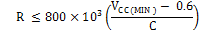
where R is the pull-up resistor value in Ω, VCC(MIN) is the minimum VCC voltage in volts, and C is the equivalent bus capacitance in picofarads (pF).

In addition, regardless of the bus capacitance, always choose RPU ≤ 65.7 kΩ for VCC = 5.5 V, RPU ≤ 45 kΩ for VCC = 3.3 V, and RPU ≤ 33 kΩ for VCC = 2.5 V. The start-up circuitry requires logic HIGH voltages on SDAOUT and SCLOUT to connect the backplane to the card, and these pull-up values are needed to overcome the pre-charge voltage.