SCPS200E July   2009  – April 2019 TCA9555

PRODUCTION DATA.  

  1. Features
  2. Applications
  3. Description
    1.     Device Images
      1.      Simplified Schematic
  4. Revision History
  5. Description (continued)
  6. Pin Configuration and Functions
    1.     Pin Functions
  7. Specifications
    1. 7.1 Absolute Maximum Ratings
    2. 7.2 ESD Ratings
    3. 7.3 Recommended Operating Conditions
    4. 7.4 Thermal Information
    5. 7.5 Electrical Characteristics
    6. 7.6 I2C Interface Timing Requirements
    7. 7.7 Switching Characteristics
    8. 7.8 Typical Characteristics
  8. Parameter Measurement Information
  9. Detailed Description
    1. 9.1 Overview
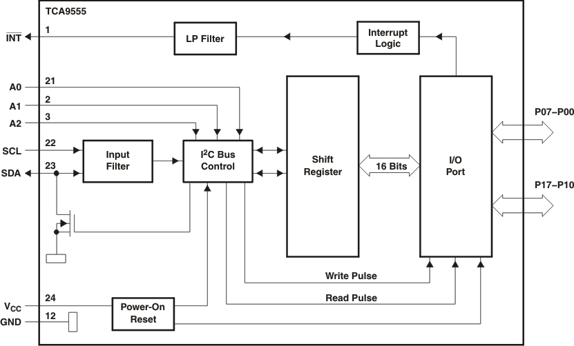
    2. 9.2 Functional Block Diagram
    3. 9.3 Feature Description
      1. 9.3.1 5-V Tolerant I/O Ports
      2. 9.3.2 Hardware Address Pins
      3. 9.3.3 Interrupt (INT) Output
    4. 9.4 Device Functional Modes
      1. 9.4.1 Power-On Reset (POR)
      2. 9.4.2 Powered-Up
    5. 9.5 Programming
      1. 9.5.1 I/O Port
      2. 9.5.2 I2C Interface
        1. 9.5.2.1 Bus Transactions
          1. 9.5.2.1.1 Writes
          2. 9.5.2.1.2 Reads
      3. 9.5.3 Device Address
      4. 9.5.4 Control Register and Command Byte
    6. 9.6 Register Maps
      1. 9.6.1 Register Descriptions
  10. 10Application and Implementation
    1. 10.1 Application Information
    2. 10.2 Typical Application
      1. 10.2.1 Design Requirements
      2. 10.2.2 Detailed Design Procedure
        1. 10.2.2.1 Calculating Junction Temperature and Power Dissipation
        2. 10.2.2.2 Minimizing ICC When I/O Is Used to Control LED
        3. 10.2.2.3 Pull-Up Resistor Calculation
      3. 10.2.3 Application Curves
  11. 11Power Supply Recommendations
  12. 12Layout
    1. 12.1 Layout Guidelines
    2. 12.2 Layout Example
  13. 13Device and Documentation Support
    1. 13.1 Documentation Support
      1. 13.1.1 Related Documentation
    2. 13.2 Receiving Notification of Documentation Updates
    3. 13.3 Community Resources
    4. 13.4 Trademarks
    5. 13.5 Electrostatic Discharge Caution
    6. 13.6 Glossary
  14. 14Mechanical, Packaging, and Orderable Information

Package Options

Mechanical Data (Package|Pins)
Thermal pad, mechanical data (Package|Pins)
Orderable Information

Functional Block Diagram

TCA9555 ld_cps200.gif
Pin numbers shown are for the PW package.
All I/Os are set to inputs at reset.
Figure 22. Logic Diagram (Positive Logic)