SLLSES9D February   2016  – October 2021 TCAN1042-Q1 , TCAN1042G-Q1 , TCAN1042GV-Q1 , TCAN1042H-Q1 , TCAN1042HG-Q1 , TCAN1042HGV-Q1 , TCAN1042HV-Q1 , TCAN1042V-Q1

PRODUCTION DATA  

  1. Features
  2. Applications
  3. Description
  4. Revision History
  5. Device Comparison Table
  6. Pin Configurations and Functions
  7. Specifications
    1. 7.1 Absolute Maximum Ratings
    2. 7.2 ESD Ratings
    3. 7.3 ESD Ratings, Specifications
    4. 7.4 Recommended Operating Conditions
    5. 7.5 Thermal Information
    6. 7.6 Power Rating
    7. 7.7 Electrical Characteristics
    8. 7.8 Switching Characteristics
    9. 7.9 Typical Characteristics
  8. Parameter Measurement Information
  9. Detailed Description
    1. 9.1 Overview
    2. 9.2 Functional Block Diagram
    3. 9.3 Feature Description
      1. 9.3.1 TXD Dominant Timeout (DTO)
      2. 9.3.2 Thermal Shutdown (TSD)
      3. 9.3.3 Undervoltage Lockout
      4. 9.3.4 Unpowered Device
      5. 9.3.5 Floating Terminals
      6. 9.3.6 CAN Bus Short Circuit Current Limiting
      7. 9.3.7 Digital Inputs and Outputs
        1. 9.3.7.1 Devices with VCC Only (Devices without the "V" Suffix):
        2. 9.3.7.2 Devices with VIO I/O Level Shifting (Devices with "V" Suffix):
    4. 9.4 Device Functional Modes
      1. 9.4.1 CAN Bus States
      2. 9.4.2 Normal Mode
      3. 9.4.3 Standby Mode
        1. 9.4.3.1 Remote Wake Request via Wake Up Pattern (WUP) in Standby Mode
      4. 9.4.4 Driver and Receiver Function Tables
  10. 10Application Information Disclaimer
    1. 10.1 Application Information
    2. 10.2 Typical Applications
      1. 10.2.1 Design Requirements
        1. 10.2.1.1 Bus Loading, Length and Number of Nodes
      2. 10.2.2 Detailed Design Procedures
        1. 10.2.2.1 CAN Termination
      3. 10.2.3 Application Curves
  11. 11Power Supply Recommendations
  12. 12Device and Documentation Support
    1. 12.1 Receiving Notification of Documentation Updates
    2. 12.2 Support Resources
    3. 12.3 Trademarks
    4. 12.4 Electrostatic Discharge Caution
    5. 12.5 Glossary
  13. 13Mechanical, Packaging, and Orderable Information

Package Options

Mechanical Data (Package|Pins)
Thermal pad, mechanical data (Package|Pins)
Orderable Information

Description

This CAN transceiver family meets the ISO11898-2 (2016) High Speed CAN (Controller Area Network) physical layer standard. All devices are designed for use in CAN FD networks up to 2 Mbps (megabits per second). Devices with part numbers that include the "G" suffix are designed for data rates up to 5 Mbps, and versions with the "V" have a secondary power supply input for I/O level shifting the input pin thresholds and RXD output level. This family has a low power standby mode with remote wake request feature. Additionally, all devices include many protection features to enhance device and network robustness.

Device Information
PART NUMBERPACKAGE(1)BODY SIZE
TCAN1042x-Q1SOIC (8)4.90 mm × 3.91 mm
VSON (8)3.00 mm x 3.00 mm
For all available packages, see the orderable addendum at the end of the data sheet.
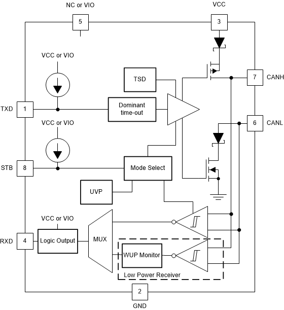
GUID-BC366BBE-09E5-4A7E-AA88-E9538D5568EF-low.gif
Terminal 5 function is device dependent; NC on devices without the "V" suffix, and VIO for I/O level shifting for devices with the "V" suffix.
RXD logic output is driven to VCC on devices without the "V" suffix, and VIO for devices with the "V" suffix.
Functional Block Diagram