SLOS382E September 2001 – May 2015 THS3122 , THS3125
PRODUCTION DATA.
- 1 Features
- 2 Applications
- 3 Description
- 4 Revision History
- 5 Device Options
- 6 Pin Configuration and Functions
-
7 Specifications
- 7.1 Absolute Maximum Ratings
- 7.2 Dissipation Ratings Table
- 7.3 Recommended Operating Conditions
- 7.4 Electrical Characteristics: Dynamic Performance
- 7.5 Electrical Characteristics: Noise and Distortion Performance
- 7.6 Electrical Characteristics: DC Performance
- 7.7 Electrical Characteristics: Input Characteristics
- 7.8 Electrical Characteristics: Output Characteristics
- 7.9 Electrical Characteristics: Power Supply
- 7.10 Electrical Characteristics: Shutdown Characteristics (THS3125 Only)
- 7.11 Typical Characteristics: Table Of Graphs
- 7.12 Typical Characteristics
- 8 Detailed Description
- 9 Application and Implementation
- 10Layout
- 11Device and Documentation Support
- 12Mechanical, Packaging, and Orderable Information
Package Options
Mechanical Data (Package|Pins)
Thermal pad, mechanical data (Package|Pins)
- PWP|14
Orderable Information
1 Features
- Low Noise:
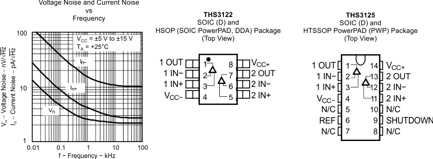
- 2.9-pA/√Hz Noninverting Current Noise
- 10.8-pA/√Hz Inverting Current Noise
- 2.2-nV/√Hz Voltage Noise
- 128-MHz , –3-dB BW (RL = 50 Ω, RF = 470 Ω)
- 1550-V/µs Slew Rate (G = 2, RL= 50Ω )
- High Output Current: 450 mA
- High Speed:
- 128-MHz , –3-dB BW (RL = 50 Ω, RF = 470 Ω)
- 1550-V/µs Slew Rate (G = 2, RL= 50Ω )
- 26-VPP Output Voltage, RL= 50 Ω
- –80 dBc (1 MHz, 2 VPP, G = 2)
- Wide Output Swing:
- 26-VPP Output Voltage, RL= 50 Ω
- –80 dBc (1 MHz, 2 VPP, G = 2)
- 370-µA Shutdown Supply Current
- Low Distortion:
- –80 dBc (1 MHz, 2 VPP, G = 2)
- 370-µA Shutdown Supply Current
- Low-Power Shutdown Mode (THS3125)
- 370-µA Shutdown Supply Current
- Standard SOIC, HSOP PowerPAD™, and HTSSOP PowerPAD Packages
2 Applications
- Video Distribution
- Instrumentation
- Line Drivers
- Motor Drivers
- Piezo Drivers
3 Description
The THS3122 and THS3125 are low-noise, high-speed current feedback amplifiers, with high output current drive. This makes them ideal for any application that requires low distortion over a wide frequency with heavy loads. The THS3122 and THS3125 can drive four serially-terminated video lines while maintaining a differential gain error less than 0.03%.
The high output drive capability of the THS3122 and THS3125 enables the devices to drive 50-Ω loads with low distortion over a wide range of output voltages:
- –80-dBc THD at 2 VPP
- –75-dBc THD at 8 VPP
The THS3122 and THS3125 operate from ±5-V to ±15-V supply voltages while drawing as little as 7.2 mA of supply current per channel. The THS3125 offers a low-power shutdown mode, reducing the supply current to only 370 µA. The THS3122 and THS3125 are packaged in SOIC, HSOP, and HTSSOP packages.
Device Information(1)
| PART NUMBER | PACKAGE | BODY SIZE (NOM) |
|---|---|---|
| THS3122 | SOIC (8) | 4.90 mm × 3.91 mm |
| HSOP (8) | 4.89 mm × 3.90 mm | |
| THS3125 | SOIC (14) | 8.65 mm × 3.91 mm |
| HTSSOP (14) | 5.00 mm × 4.40 mm |
- For all available packages, see the package option addendum at the end of the data sheet.
4 Revision History
Changes from D Revision (February 2011) to E Revision
- Added missing minus sign to temperature range in Available Options table Go
- Changed Input Offset parameter maximum values in Electrical Charateristics for DC PerformanceGo
- Added Detailed Description sectionGo
- Added Application and Implementation sectionGo
- Change Application Information sectionGo
Changes from C Revision (July 2010) to D Revision
- Changed output current (absolute maximum) from 275 mA to 550 mAGo
Changes from B Revision (October, 2009) to C Revision
- Corrected REF pin name for THS3125 shown in front-page figureGo
- Deleted Shutdown pin input levels parameters and specifications from Recommended Operating Conditions tableGo
- Updated Shutdown Characteristics table test conditions; changed GND to REF, corrected VSHDN notationsGo
- Added VREF and VSHDN parameters and speciifications to Shutdown Characteristics tableGo
- Revised second and fourth paragraphs of Saving Power with Shutdown Functionality sectionGo
- Updated equation in Power-Down Reference Pin Operation section that describes usable range at the REF pinGo
- Revised paragraph in Power-Down Reference Pin Operation that discusses behavior of unterminated REF pinGo
