SLOS382E September 2001 – May 2015 THS3122 , THS3125
PRODUCTION DATA.
- 1 Features
- 2 Applications
- 3 Description
- 4 Revision History
- 5 Device Options
- 6 Pin Configuration and Functions
-
7 Specifications
- 7.1 Absolute Maximum Ratings
- 7.2 Dissipation Ratings Table
- 7.3 Recommended Operating Conditions
- 7.4 Electrical Characteristics: Dynamic Performance
- 7.5 Electrical Characteristics: Noise and Distortion Performance
- 7.6 Electrical Characteristics: DC Performance
- 7.7 Electrical Characteristics: Input Characteristics
- 7.8 Electrical Characteristics: Output Characteristics
- 7.9 Electrical Characteristics: Power Supply
- 7.10 Electrical Characteristics: Shutdown Characteristics (THS3125 Only)
- 7.11 Typical Characteristics: Table Of Graphs
- 7.12 Typical Characteristics
- 8 Detailed Description
- 9 Application and Implementation
- 10Layout
- 11Device and Documentation Support
- 12Mechanical, Packaging, and Orderable Information
Package Options
Mechanical Data (Package|Pins)
Thermal pad, mechanical data (Package|Pins)
- PWP|14
Orderable Information
10 Layout
10.1 Layout Guidelines
10.1.1 Printed-Circuit Board Layout Techniques For Optimal Performance
Achieving optimum performance with high-frequency amplifiers such as the THS3125 and THS3122 requires careful attention to board layout parasitic and external component types. Recommendations that optimize performance include:
- Minimize parasitic capacitance to any ac ground for all of the signal I/O pins. Parasitic capacitance on the output and input pins can cause instability. To reduce unwanted capacitance, a window around the signal I/O pins should be opened in all of the ground and power planes around those pins. Otherwise, ground and power planes should be unbroken elsewhere on the board.
- Minimize the distance [0.25 inch, (6,4 mm)] from the power-supply pins to high-frequency 0.1-µF and 100-pF decoupling capacitors. At the device pins, the ground and power plane layout should not be in close proximity to the signal I/O pins. Avoid narrow power and ground traces to minimize inductance between the pins and the decoupling capacitors. The power-supply connections should always be decoupled with these capacitors. Larger (6.8 µF or more) tantalum decoupling capacitors, effective at lower frequencies, should also be used on the main supply pins. These capacitors may be placed somewhat farther from the device and may be shared among several devices in the same area of the printed circuit board (PCB).
- Careful selection and placement of external components preserve the high-frequency performance of the THS3125 and THS3122. Resistors should be a very low reactance type. Surface-mount resistors work best and allow a tighter overall layout. Again, keep the leads and PCB trace length as short as possible. Never use wirebound type resistors in a high-frequency application. Because the output pin and inverting input pins are the most sensitive to parasitic capacitance, always position the feedback and series output resistors, if any, as close as possible to the inverting input pins and output pins. Other network components, such as input termination resistors, should be placed close to the gain-setting resistors. Even with a low parasitic capacitance that shunts the external resistors, excessively high resistor values can create significant time constants that can degrade performance. Good axial metal-film or surface-mount resistors have approximately 0.2 pF in shunt with the resistor. For resistor values greater than 2.0 kΩ, this parasitic capacitance can add a pole and/or a zero that can affect circuit operation. Keep resistor values as low as possible, consistent with load driving considerations.
- Connections to other wideband devices on the board may be made with short direct traces or through onboard transmission lines. For short connections, consider the trace and the input to the next device as a lumped capacitive load. Relatively wide traces [0.05 inch (1,3 mm) to 0.1 inch (2,54 mm)] should be used, preferably with ground and power planes opened up around them. Estimate the total capacitive load and determine if isolation resistors on the outputs are necessary. Low parasitic capacitive loads (less than 4 pF) may not need an RS because the THS3125 and THS3122 are nominally compensated to operate with a 2-pF parasitic load. Higher parasitic capacitive loads without an RS are allowed as the signal gain increases (thus increasing the unloaded phase margin). If a long trace is required, and the 6-dB signal loss intrinsic to a doubly-terminated transmission line is acceptable, implement a matched-impedance transmission line using microstrip or stripline techniques (consult an ECL design handbook for microstrip and stripline layout techniques). A 50-Ω environment is not necessary onboard, and in fact, a higher impedance environment improves distortion as shown in the distortion versus load plots. With a characteristic board trace impedance based on board material and trace dimensions, a matching series resistor into the trace from the output of the THS3125/THS3122 is used as well as a terminating shunt resistor at the input of the destination device. Remember also that the terminating impedance is the parallel combination of the shunt resistor and the input impedance of the destination device: this total effective impedance should be set to match the trace impedance. If the 6-dB attenuation of a doubly-terminated transmission line is unacceptable, a long trace can be series-terminated at the source end only. Treat the trace as a capacitive load in this case. This configuration does not preserve signal integrity as well as a doubly-terminated line. If the input impedance of the destination device is low, there is some signal attenuation as a result of the voltage divider formed by the series output into the terminating impedance.
- Socketing a high-speed device such as the THS3125 and THS3122 is not recommended. The additional lead length and pin-to-pin capacitance introduced by the socket can create an extremely troublesome parasitic network which can make it almost impossible to achieve a smooth, stable frequency response. Best results are obtained by soldering the THS3125/THS3122 amplifiers directly onto the board.
10.1.2 PowerPAD Design Considerations
The THS3125 and THS3122 are available in a thermally-enhanced PowerPAD family of packages. These packages are constructed using a downset leadframe upon which the die is mounted [see Figure 48(a) and Figure 48(b)]. This arrangement results in the lead frame being exposed as a thermal pad on the underside of the package [see Figure 48(c)]. Because this thermal pad has direct thermal contact with the die, excellent thermal performance can be achieved by providing a good thermal path away from the thermal pad. Note that devices such as the THS312x have no electrical connection between the PowerPAD and the die.
 Figure 48. Views Of Thermally-Enhanced Package
The PowerPAD package allows for both assembly and thermal management in one manufacturing operation. During the surface-mount solder operation (when the leads are being soldered), the thermal pad can also be soldered to a copper area underneath the package. Through the use of thermal paths within this copper area, heat can be conducted away from the package into either a ground plane or other heat dissipating device.
The PowerPAD package represents a breakthrough in combining the small area and ease of assembly of surface mount with the, heretofore, awkward mechanical methods of heatsinking.
10.1.3 PowerPAD Layout Considerations

NOINDENT:
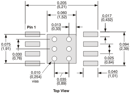
Dimensions are in inches (millimeters).Although there are many ways to properly heatsink the PowerPAD package, the following steps illustrate the recommended approach.
- PCB with a top side etch pattern as shown in Figure 49.
- Place five holes in the area of the thermal pad. These holes should be 0.01 inch (0,254 mm) in diameter. Keep them small so that solder wicking through the holes is not a problem during reflow.
- Additional vias may be placed anywhere along the thermal plane outside of the thermal pad area. These vias help dissipate the heat generated by the THS3125/THS3122 IC. These additional vias may be larger than the 0.01-inch (0,254-mm) diameter vias directly under the thermal pad. They can be larger because they are not in the thermal pad area to be soldered so that wicking is not a problem.
- Connect all holes to the internal ground plane. Note that the PowerPAD is electrically isolated from the silicon and all leads. Connecting the PowerPAD to any potential voltage, such as VS–, is acceptable as there is no electrical connection to the silicon.
- When connecting these holes to the ground plane, do not use the typical web or spoke via connection methodology. Web connections have a high thermal resistance connection that is useful for slowing the heat transfer during soldering operations. This resistance makes the soldering of vias that have plane connections easier. In this application; however, low thermal resistance is desired for the most efficient heat transfer. Therefore, the holes under the THS3125/THS3122 PowerPAD package should make the connection to the internal ground plane with a complete connection around the entire circumference of the plated-through hole.
- The top-side solder mask should leave the terminals of the package and the thermal pad area with its five holes exposed. The bottom-side solder mask should cover the five holes of the thermal pad area. This configuration prevents solder from being pulled away from the thermal pad area during the reflow process.
- Apply solder paste to the exposed thermal pad area and all of the IC terminals.
- With these preparatory steps in place, the IC is simply placed in position and run through the solder reflow operation as any standard surface-mount component. This procedure results in a part that is properly installed.
10.1.4 Power Dissipation And Thermal Considerations
The THS3125 and THS3122 incorporate automatic thermal shutoff protection. This protection circuitry shuts down the amplifier if the junction temperature exceeds approximately +160°C. When the junction temperature reduces to approximately +140°C, the amplifier turns on again. However, for maximum performance and reliability, the designer must take care to ensure that the design does not exceed a junction temperature of +125°C. Between +125°C and +150°C, damage does not occur, but the performance of the amplifier begins to degrade and long-term reliability suffers. The thermal characteristics of the device are dictated by the package and the PCB. Maximum power dissipation for a given package can be calculated using the following formula.

where
- PDMax is the maximum power dissipation in the amplifier (W)
- Tmax is the absolute maximum junction temperature (°C)
- TA is the ambient temperature (°C)
where
- θJC is the thermal coefficient from the silicon junctions to the case (°C/W)
- θCA is the thermal coefficient from the case to ambient air (°C/W)
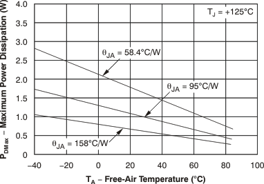
For systems where heat dissipation is more critical, the THS3125 and THS3122 are also available in an 8-pin MSOP with PowerPAD package that offers even better thermal performance. The thermal coefficient for the PowerPAD packages are substantially improved over the traditional SOIC. Maximum power dissipation levels are depicted in Figure 50 for the available packages. The data for the PowerPAD packages assume a board layout that follows the PowerPAD layout guidelines discussed above and detailed in the PowerPAD application note (literature number SLMA002). Figure 50 also illustrates the effect of not soldering the PowerPAD to a PCB. The thermal impedance increases substantially, which may cause serious heat and performance issues. Always solder the PowerPAD to the PCB for optimum performance.

NOINDENT:
Results shown are with no air flow and PCB size of 3 in × 3 in (76,2 mm × 76,2 mm).- θJA = 58.4°C/W for 8-pin MSOP with PowerPAD (DGN package)
- θJA = 95°C/W for 8-pin SOIC High-K test PCB (D package)
- θJA = 158°C/W for 8-pin MSOP with PowerPAD without solder
When determining whether or not the device satisfies the maximum power dissipation requirement, it is important to not only consider quiescent power dissipation, but also dynamic power dissipation. Often times, this type of dissipation is difficult to quantify because the signal pattern is inconsistent, but an estimate of the RMS power dissipation can provide visibility into a possible problem.