SCPS260C August   2017  – February 2022 TIC12400-Q1

PRODUCTION DATA  

  1. Features
  2. Applications
  3. Description
  4. Revision History
  5. Pin Configuration and Functions
  6. Specifications
    1. 6.1 Absolute Maximum Ratings
    2. 6.2 ESD Ratings
    3. 6.3 Recommended Operating Conditions
    4. 6.4 Thermal Information
    5. 6.5 Electrical Characteristics
    6. 6.6 Timing Requirements
    7. 6.7 Typical Characteristics
  7. Parameter Measurement Information
  8. Detailed Description
    1. 8.1 Overview
    2. 8.2 Functional Block Diagram
    3. 8.3 Feature Description
      1. 8.3.1  VS Pin
      2. 8.3.2  VDD Pin
      3. 8.3.3  Device Initialization
      4. 8.3.4  Device Trigger
      5. 8.3.5  Device Reset
        1. 8.3.5.1 VS Supply POR
        2. 8.3.5.2 Hardware Reset
        3. 8.3.5.3 Software Reset
      6. 8.3.6  VS Under-Voltage (UV) Condition
      7. 8.3.7  VS Over-Voltage (OV) Condition
      8. 8.3.8  Switch Inputs Settings
        1. 8.3.8.1 Input Current Source and Sink Selection
        2. 8.3.8.2 Input Mode Selection
        3. 8.3.8.3 Input Enable Selection
        4. 8.3.8.4 Thresholds Adjustment
        5. 8.3.8.5 Wetting Current Configuration
      9. 8.3.9  Interrupt Generation and INT Assertion
        1. 8.3.9.1 INT Pin Assertion Scheme
        2. 8.3.9.2 Interrupt Idle Time (tINT_IDLE) Time
        3. 8.3.9.3 Microcontroller Wake-Up
        4. 8.3.9.4 Interrupt Enable or Disable and Interrupt Generation Conditions
        5. 8.3.9.5 Detection Filter
      10. 8.3.10 Temperature Monitor
        1. 8.3.10.1 Temperature Warning (TW)
        2. 8.3.10.2 Temperature Shutdown (TSD)
      11. 8.3.11 Parity Check and Parity Generation
      12. 8.3.12 Cyclic Redundancy Check (CRC)
    4. 8.4 Device Functional Modes
      1. 8.4.1 Continuous Mode
      2. 8.4.2 Polling Mode
        1. 8.4.2.1 Standard Polling
        2. 8.4.2.2 Matrix polling
      3. 8.4.3 Additional Features
        1. 8.4.3.1 Clean Current Polling (CCP)
        2. 8.4.3.2 Wetting Current Auto-Scaling
        3. 8.4.3.3 VS Measurement
        4. 8.4.3.4 Wetting Current Diagnostic
        5. 8.4.3.5 ADC Self-Diagnostic
    5. 8.5 Programming
      1. 8.5.1 SPI Communication Interface Buses
        1. 8.5.1.1 Chip Select ( CS)
        2. 8.5.1.2 System Clock (SCLK)
        3. 8.5.1.3 Slave In (SI)
        4. 8.5.1.4 Slave Out (SO)
      2. 8.5.2 SPI Sequence
        1. 8.5.2.1 Read Operation
        2. 8.5.2.2 Write Operation
        3. 8.5.2.3 Status Flag
    6. 8.6 Register Maps
    7. 8.7 Programming Guidelines
  9. Application Information Disclaimer
    1. 9.1 Application Information
    2. 9.2 Using TIC12400-Q1 in a 12 V Automotive System
    3. 9.3 Resistor-coded Switches Detection in Automotive Body Control Module
      1. 9.3.1 Design Requirements
      2. 9.3.2 Detailed Design Procedure
      3. 9.3.3 Application Curves
  10. 10Power Supply Recommendations
  11. 11Layout
    1. 11.1 Layout Guidelines
    2. 11.2 Layout Example
  12. 12Device and Documentation Support
    1. 12.1 Receiving Notification of Documentation Updates
    2. 12.2 Support Resources
    3. 12.3 Trademarks
    4. 12.4 Electrostatic Discharge Caution
    5. 12.5 Glossary
  13. 13Mechanical, Packaging, and Orderable Information

Package Options

Mechanical Data (Package|Pins)
Thermal pad, mechanical data (Package|Pins)
Orderable Information

Interrupt Idle Time (tINT_IDLE) Time

Interrupt idle time (tINT_IDLE) is implemented in TIC12400-Q1 to:

  • Allow the INT pin enough time to be pulled back high by the external pull-up resistor and allow the next assertion to be detectable by an edge-triggered microcontroller.
  • Minimize the chance of glitching on the INT pin if back-to-back events occur.

When there is a pending interrupt event and the interrupt event is not masked, tINT_IDLE is applied after the READ command is issued to the INT_STAT register. If another event occurs during the interrupt idle time the INT_STAT register content is updated instantly but the INT pin is not asserted low until tINT_IDLE has elapsed. If another READ command is issued to the INT_STAT register during tINT_IDLE, the INT_STAT register content is cleared immediately, but the INT pin is not re-asserted back low after tINT_IDLE has elapsed. An example of the interrupt idle time is given below to illustrate the INT pin behavior under the static INT assertion schemes:
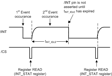
GUID-462B7504-490B-45BB-881F-044B9561DF43-low.gifFigure 8-8 INT Assertion Scheme With tINT_IDLE