SCPS260C August 2017 – February 2022 TIC12400-Q1
PRODUCTION DATA
- 1 Features
- 2 Applications
- 3 Description
- 4 Revision History
- 5 Pin Configuration and Functions
- 6 Specifications
- 7 Parameter Measurement Information
-
8 Detailed Description
- 8.1 Overview
- 8.2 Functional Block Diagram
- 8.3
Feature Description
- 8.3.1 VS Pin
- 8.3.2 VDD Pin
- 8.3.3 Device Initialization
- 8.3.4 Device Trigger
- 8.3.5 Device Reset
- 8.3.6 VS Under-Voltage (UV) Condition
- 8.3.7 VS Over-Voltage (OV) Condition
- 8.3.8 Switch Inputs Settings
- 8.3.9 Interrupt Generation and INT Assertion
- 8.3.10 Temperature Monitor
- 8.3.11 Parity Check and Parity Generation
- 8.3.12 Cyclic Redundancy Check (CRC)
- 8.4 Device Functional Modes
- 8.5 Programming
- 8.6 Register Maps
- 8.7 Programming Guidelines
- 9 Application Information Disclaimer
- 10Power Supply Recommendations
- 11Layout
- 12Device and Documentation Support
- 13Mechanical, Packaging, and Orderable Information
Package Options
Mechanical Data (Package|Pins)
- DCP|38
Thermal pad, mechanical data (Package|Pins)
- DCP|38
Orderable Information
3 Description
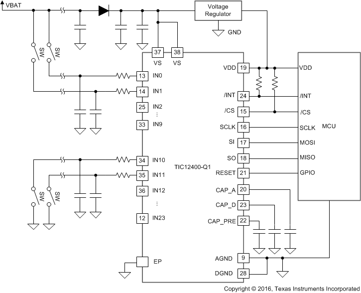
The TIC12400-Q1 is an advanced Multiple Switch Detection Interface (MSDI) designed to detect external switch status in a 12-V automotive system. The TIC12400-Q1 features an integrated 10-bit ADC to monitor multi-position analog switches and a comparator to monitor digital switches independently of the MCU. Detection thresholds can be programmed for the ADC and the comparator to support various switch topologies and system non-idealities. The device monitors 24 direct switch inputs, with 10 inputs configurable to monitor switches connected to either ground or battery. 6 unique wetting current settings can be programmed for each input to support different application scenarios. The device supports wake-up operation on all switch inputs to eliminate the need to keep the MCU active continuously, thus reducing power consumption of the system. The TIC12400-Q1 also offers integrated fault detection, ESD protection, and diagnostic functions for improved system robustness. The TIC12400-Q1 supports 2 modes of operations: continuous and polling mode. In continuous mode, wetting current is supplied continuously. In polling mode, wetting current is turned on periodically to sample the input status based on a programmable timer, thus the system power consumption is significantly reduced.
| PART NUMBER | PACKAGE(1) | BODY SIZE (NOM) |
|---|---|---|
| TIC12400-Q1 | TSSOP (38) | 9.70 mm × 4.40 mm |
 Simplified Schematic