SLLSEV5D July 2017 – June 2019 TIOL111 , TIOL1113 , TIOL1115
PRODUCTION DATA.
- 1 Features
- 2 Applications
- 3 Description
- 4 Revision History
- 5 Pin Configuration and Functions
- 6 Specifications
- 7 Parameter Measurement Information
-
8 Detailed Description
- 8.1 Overview
- 8.2 Functional Block Diagrams
- 8.3
Feature Description
- 8.3.1 Wake Up Detection
- 8.3.2 Current Limit Configuration
- 8.3.3 Current Fault Detection, Indication and Auto Recovery
- 8.3.4 Thermal Warning, Thermal Shutdown
- 8.3.5 Fault Reporting (NFAULT)
- 8.3.6 Transceiver Function Tables
- 8.3.7 The Integrated Voltage Regulator (LDO)
- 8.3.8 Reverse Polarity Protection
- 8.3.9 Integrated Surge Protection and Transient Waveform Tolerance
- 8.3.10 Power Up Sequence (TIOL111)
- 8.3.11 Undervoltage Lock-Out (UVLO)
- 8.4 Device Functional Modes
- 9 Application and Implementation
- 10Power Supply Recommendations
- 11Layout
- 12Device and Documentation Support
- 13Mechanical, Packaging, and Orderable Information
Package Options
Mechanical Data (Package|Pins)
- DMW|10
Thermal pad, mechanical data (Package|Pins)
Orderable Information
9.2.2.3 Driving Inductive Loads
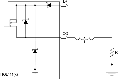
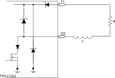
The TIOL111(x) family is capable of magnetizing and demagnetizing inductive loads up to 1.5H. These devices contain internal circuitry that enables fast demagnetization when configured as either P-switch or N-switch mode.
In P-switch configuration, the load inductor L is magnetized when the CQ output is driven high. When the PNP is turned off, there is a significant amount of negative inductive kick back at the CQ pin. This voltage is clamped internally at about -75 V.
Similarly in N-switch configuration, the load inductor L is magnetized when the CQ output is driven low. When the NPN is turned off, there is a significant amount of positive inductive kick back at the CQ pin. This voltage is clamped internally at about 75 V.
The equivalent protection circuits are shown in Figure 18 and Figure 19. The minimum value of the resistive load R can be calculated as:

 Figure 18. P-Switch Mode
  Figure 19. N-Switch Mode