SBAS980B June   2019  – June 2020 TLA2518

PRODUCTION DATA.  

  1. Features
  2. Applications
  3. Description
    1.     Device Images
      1.      TLA2518 Block Diagram and Applications
  4. Revision History
  5. Pin Configuration and Functions
    1.     Pin Functions
  6. Specifications
    1. 6.1 Absolute Maximum Ratings
    2. 6.2 ESD Ratings
    3. 6.3 Recommended Operating Conditions
    4. 6.4 Thermal Information
    5. 6.5 Electrical Characteristics
    6. 6.6 Timing Requirements
    7. 6.7 Switching Characteristics
    8. 6.8 Typical Characteristics
  7. Detailed Description
    1. 7.1 Overview
    2. 7.2 Functional Block Diagram
    3. 7.3 Feature Description
      1. 7.3.1 Multiplexer and ADC
      2. 7.3.2 Reference
      3. 7.3.3 ADC Transfer Function
      4. 7.3.4 ADC Offset Calibration
      5. 7.3.5 Programmable Averaging Filter
      6. 7.3.6 General-Purpose I/Os
      7. 7.3.7 Oscillator and Timing Control
      8. 7.3.8 Output Data Format
      9. 7.3.9 Device Programming
        1. 7.3.9.1 Enhanced-SPI Interface
        2. 7.3.9.2 Register Read/Write Operation
          1. 7.3.9.2.1 Register Write
          2. 7.3.9.2.2 Register Read
    4. 7.4 Device Functional Modes
      1. 7.4.1 Device Power-Up and Reset
      2. 7.4.2 Manual Mode
      3. 7.4.3 On-the-Fly Mode
      4. 7.4.4 Auto-Sequence Mode
    5. 7.5 TLA2518 Registers
      1. 7.5.1  SYSTEM_STATUS Register (Address = 0x0) [reset = 0x81]
        1. Table 9. SYSTEM_STATUS Register Field Descriptions
      2. 7.5.2  GENERAL_CFG Register (Address = 0x1) [reset = 0x0]
        1. Table 10. GENERAL_CFG Register Field Descriptions
      3. 7.5.3  DATA_CFG Register (Address = 0x2) [reset = 0x0]
        1. Table 11. DATA_CFG Register Field Descriptions
      4. 7.5.4  OSR_CFG Register (Address = 0x3) [reset = 0x0]
        1. Table 12. OSR_CFG Register Field Descriptions
      5. 7.5.5  OPMODE_CFG Register (Address = 0x4) [reset = 0x0]
        1. Table 13. OPMODE_CFG Register Field Descriptions
      6. 7.5.6  PIN_CFG Register (Address = 0x5) [reset = 0x0]
        1. Table 14. PIN_CFG Register Field Descriptions
      7. 7.5.7  GPIO_CFG Register (Address = 0x7) [reset = 0x0]
        1. Table 15. GPIO_CFG Register Field Descriptions
      8. 7.5.8  GPO_DRIVE_CFG Register (Address = 0x9) [reset = 0x0]
        1. Table 16. GPO_DRIVE_CFG Register Field Descriptions
      9. 7.5.9  GPO_VALUE Register (Address = 0xB) [reset = 0x0]
        1. Table 17. GPO_VALUE Register Field Descriptions
      10. 7.5.10 GPI_VALUE Register (Address = 0xD) [reset = 0x0]
        1. Table 18. GPI_VALUE Register Field Descriptions
      11. 7.5.11 SEQUENCE_CFG Register (Address = 0x10) [reset = 0x0]
        1. Table 19. SEQUENCE_CFG Register Field Descriptions
      12. 7.5.12 CHANNEL_SEL Register (Address = 0x11) [reset = 0x0]
        1. Table 20. CHANNEL_SEL Register Field Descriptions
      13. 7.5.13 AUTO_SEQ_CH_SEL Register (Address = 0x12) [reset = 0x0]
        1. Table 21. AUTO_SEQ_CH_SEL Register Field Descriptions
  8. Application and Implementation
    1. 8.1 Application Information
    2. 8.2 Typical Applications
      1. 8.2.1 Mixed-Channel Configuration
        1. 8.2.1.1 Design Requirements
        2. 8.2.1.2 Detailed Design Procedure
          1. 8.2.1.2.1 Digital Input
          2. 8.2.1.2.2 Digital Open-Drain Output
        3. 8.2.1.3 Application Curve
      2. 8.2.2 Digital Push-Pull Output Configuration
  9. Power Supply Recommendations
    1. 9.1 AVDD and DVDD Supply Recommendations
  10. 10Layout
    1. 10.1 Layout Guidelines
    2. 10.2 Layout Example
  11. 11Device and Documentation Support
    1. 11.1 Receiving Notification of Documentation Updates
    2. 11.2 Support Resources
    3. 11.3 Trademarks
    4. 11.4 Electrostatic Discharge Caution
    5. 11.5 Glossary
  12. 12Mechanical, Packaging, and Orderable Information

Package Options

Mechanical Data (Package|Pins)
Thermal pad, mechanical data (Package|Pins)
Orderable Information

Programmable Averaging Filter

The TLA2518 features a built-in oversampling (OSR) function that can be used to average several samples. The averaging filter can be enabled by programming the OSR[2:0] bits in the OSR_CFG register. The averaging filter configuration is common to all analog input channels. Figure 24 shows that the averaging filter module output is 16 bits long. In manual conversion mode and auto-sequence mode, only the first conversion for the selected analog input channel must be initiated by the host; see the Manual Mode and Auto-Sequence Mode sections. As shown in Figure 24, any remaining conversions for the selected averaging factor are generated internally. The time required to complete the averaging operation is determined by the sampling speed and number of samples to be averaged. As shown in Figure 24, the 16-bit result can be read out after the averaging operation completes.
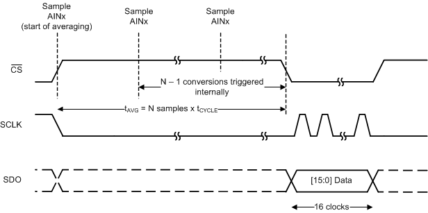
TLA2518 osr_conversion.gifFigure 24. Averaging Example

Equation 2 provides the LSB value of the 16-bit average result.

Equation 2. TLA2518 eq_lsb_high_prec_data_sbas773.gif