SBAS961A May   2019  – April 2020 TLA2528

PRODUCTION DATA.  

  1. Features
  2. Applications
  3. Description
    1.     Device Images
      1.      TLA2528 Block Diagram and Applications
  4. Revision History
  5. Pin Configuration and Functions
    1.     Pin Functions
  6. Specifications
    1. 6.1      Absolute Maximum Ratings
    2. 6.2      ESD Ratings
    3. 6.3      Recommended Operating Conditions
    4. 6.4      Thermal Information
    5. 6.5      Electrical Characteristics
    6. Table 1. I2C Timing Requirements
    7. Table 2. Timing Requirements
    8. Table 3. I2C Switching Characteristics
    9. 6.6      Switching Characteristics
    10. 6.7      Typical Characteristics
  7. Detailed Description
    1. 7.1 Overview
    2. 7.2 Functional Block Diagram
    3. 7.3 Feature Description
      1. 7.3.1  Multiplexer and ADC
      2. 7.3.2  Reference
      3. 7.3.3  ADC Transfer Function
      4. 7.3.4  ADC Offset Calibration
      5. 7.3.5  I2C Address Selector
      6. 7.3.6  Programmable Averaging Filter
      7. 7.3.7  General-Purpose I/Os (GPIOs)
      8. 7.3.8  Oscillator and Timing Control
      9. 7.3.9  Output Data Format
      10. 7.3.10 I2C Protocol Features
        1. 7.3.10.1 General Call
        2. 7.3.10.2 General Call With Software Reset
        3. 7.3.10.3 General Call With a Software Write to the Programmable Part of the Slave Address
        4. 7.3.10.4 Configuring the Device for High-Speed I2C Mode
    4. 7.4 Device Functional Modes
      1. 7.4.1 Device Power-Up and Reset
      2. 7.4.2 Manual Mode
      3. 7.4.3 Auto-Sequence Mode
    5. 7.5 Programming
      1. 7.5.1 Reading Registers
        1. 7.5.1.1 Single Register Read
        2. 7.5.1.2 Reading a Continuous Block of Registers
      2. 7.5.2 Writing Registers
        1. 7.5.2.1 Single Register Write
        2. 7.5.2.2 Set Bit
        3. 7.5.2.3 Clear Bit
        4. 7.5.2.4 Writing a Continuous Block of Registers
    6. 7.6 TLA2528 Registers
      1. 7.6.1  SYSTEM_STATUS Register (Address = 0x0) [reset = 0x80]
        1. Table 13. SYSTEM_STATUS Register Field Descriptions
      2. 7.6.2  GENERAL_CFG Register (Address = 0x1) [reset = 0x0]
        1. Table 14. GENERAL_CFG Register Field Descriptions
      3. 7.6.3  DATA_CFG Register (Address = 0x2) [reset = 0x0]
        1. Table 15. DATA_CFG Register Field Descriptions
      4. 7.6.4  OSR_CFG Register (Address = 0x3) [reset = 0x0]
        1. Table 16. OSR_CFG Register Field Descriptions
      5. 7.6.5  OPMODE_CFG Register (Address = 0x4) [reset = 0x0]
        1. Table 17. OPMODE_CFG Register Field Descriptions
      6. 7.6.6  PIN_CFG Register (Address = 0x5) [reset = 0x0]
        1. Table 18. PIN_CFG Register Field Descriptions
      7. 7.6.7  GPIO_CFG Register (Address = 0x7) [reset = 0x0]
        1. Table 19. GPIO_CFG Register Field Descriptions
      8. 7.6.8  GPO_DRIVE_CFG Register (Address = 0x9) [reset = 0x0]
        1. Table 20. GPO_DRIVE_CFG Register Field Descriptions
      9. 7.6.9  GPO_VALUE Register (Address = 0xB) [reset = 0x0]
        1. Table 21. GPO_VALUE Register Field Descriptions
      10. 7.6.10 GPI_VALUE Register (Address = 0xD) [reset = 0x0]
        1. Table 22. GPI_VALUE Register Field Descriptions
      11. 7.6.11 SEQUENCE_CFG Register (Address = 0x10) [reset = 0x0]
        1. Table 23. SEQUENCE_CFG Register Field Descriptions
      12. 7.6.12 CHANNEL_SEL Register (Address = 0x11) [reset = 0x0]
        1. Table 24. CHANNEL_SEL Register Field Descriptions
      13. 7.6.13 AUTO_SEQ_CH_SEL Register (Address = 0x12) [reset = 0x0]
        1. Table 25. AUTO_SEQ_CH_SEL Register Field Descriptions
  8. Application and Implementation
    1. 8.1 Application Information
    2. 8.2 Typical Applications
      1. 8.2.1 Mixed-Channel Configuration
        1. 8.2.1.1 Design Requirements
        2. 8.2.1.2 Detailed Design Procedure
          1. 8.2.1.2.1 Digital Input
          2. 8.2.1.2.2 Digital Open-Drain Output
        3. 8.2.1.3 Application Curve
      2. 8.2.2 Digital Push-Pull Output
  9. Power Supply Recommendations
    1. 9.1 AVDD and DVDD Supply Recommendations
  10. 10Layout
    1. 10.1 Layout Guidelines
    2. 10.2 Layout Example
  11. 11Device and Documentation Support
    1. 11.1 Receiving Notification of Documentation Updates
    2. 11.2 Community Resources
    3. 11.3 Trademarks
    4. 11.4 Electrostatic Discharge Caution
    5. 11.5 Glossary
  12. 12Mechanical, Packaging, and Orderable Information

Package Options

Mechanical Data (Package|Pins)
Thermal pad, mechanical data (Package|Pins)
Orderable Information

Typical Characteristics

at TA = 25°C, AVDD = 5 V, DVDD = 3.3 V, and maximum throughput (unless otherwise noted)
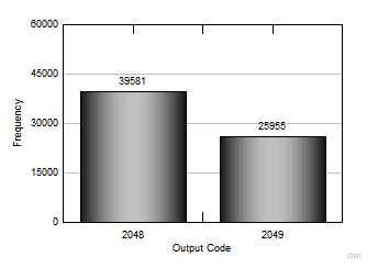
TLA2528 C001_SBAS976.gif
Standard deviation = 0.49 LSB
Figure 2. DC Input Histogram
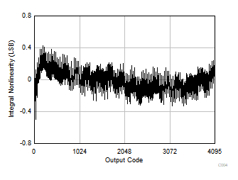
TLA2528 C004_SBAS976.gif
Typical INL = ±0.5 LSB
Figure 4. Typical INL
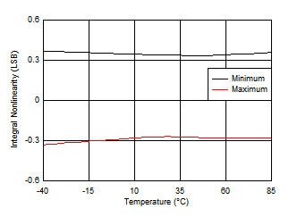
TLA2528 C005_SBAS868_SBAS961.gif
Figure 6. INL vs Temperature
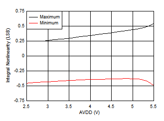
TLA2528 C019_SBAS976.gif
Figure 8. INL vs AVDD
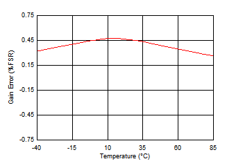
TLA2528 C007_SBAS868_SBAS961.gif
Figure 10. Gain Error vs Temperature
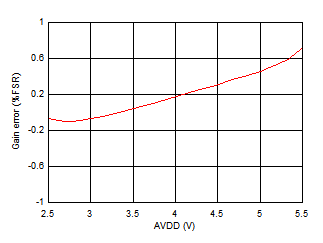
TLA2528 C017_SBAS976.gif
Figure 12. Gain Error vs AVDD
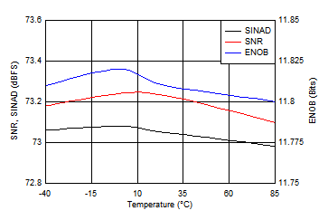
TLA2528 C009_SBAS868_SBAS961.gif
Figure 14. Noise Performance vs Temperature
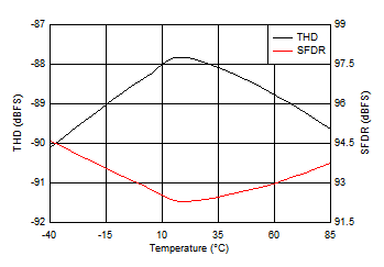
TLA2528 C011_SBAS868_SBAS961.gif
Figure 16. Distortion Performance vs Temperature
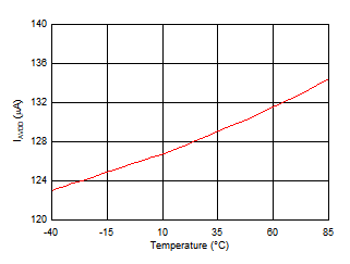
TLA2528 C013_SBAS868_SBAS961.gif
Figure 18. Analog Supply Current vs Temperature
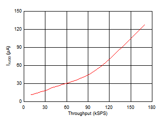
TLA2528 C015_SBAS976.gif
Figure 20. Analog Supply Current vs Throughput
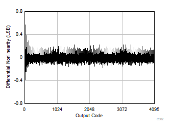
TLA2528 C002_SBAS976.gif
Typical DNL = ±0.2 LSB
Figure 3. Typical DNL
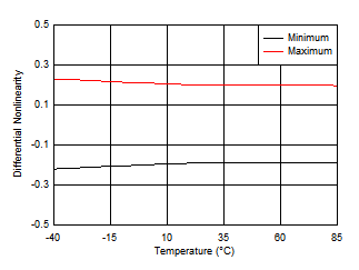
TLA2528 C003_SBAS868_SBAS961.gif
Figure 5. DNL vs Temperature
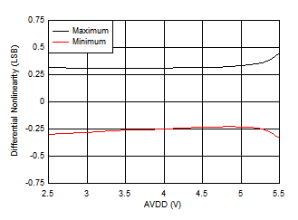
TLA2528 C018_SBAS976.gif
Figure 7. DNL vs AVDD
TLA2528 C006_SBAS868_SBAS961.gif
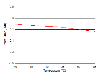
Figure 9. Offset Error vs Temperature
TLA2528 C016_SBAS976.gif
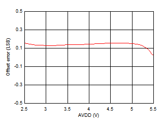
Figure 11. Offset Error vs AVDD
TLA2528 C008_SBAS976.gif
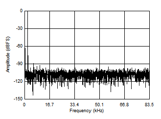
fIN = 2 kHz, SNR = 73.2 dB, THD = 92.3 dB
Figure 13. Typical FFT
TLA2528 C010_SBAS976.gif
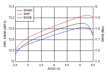
Figure 15. Noise Performance vs AVDD
TLA2528 C012_SBAS976.gif
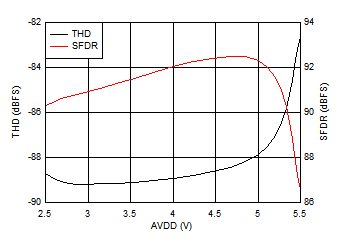
Figure 17. Distortion Performance vs AVDD
TLA2528 C014_SBAS976.gif
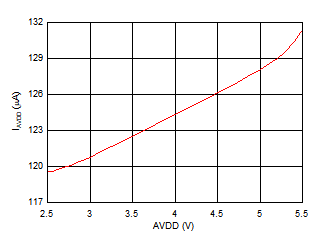
Figure 19. Analog Supply Current vs AVDD