SLFS078C October   2006  – April 2024 TLC555-Q1

PRODUCTION DATA  

  1.   1
  2. Features
  3. Applications
  4. Description
  5. Pin Configuration and Functions
  6. Specifications
    1. 5.1 Absolute Maximum Ratings
    2. 5.2 ESD Ratings
    3. 5.3 Recommended Operating Conditions
    4. 5.4 Thermal Information
    5. 5.5 Electrical Characteristics: VDD = 5 V
    6. 5.6 Electrical Characteristics: VDD = 15 V
    7. 5.7 Switching Characteristics
    8. 5.8 Typical Characteristics
  7. Detailed Description
    1. 6.1 Overview
    2. 6.2 Functional Block Diagram
    3. 6.3 Feature Description
      1. 6.3.1 Monostable Operation
      2. 6.3.2 Astable Operation
      3. 6.3.3 Frequency Divider
    4. 6.4 Device Functional Modes
  8. Application and Implementation
    1. 7.1 Application Information
    2. 7.2 Typical Applications
      1. 7.2.1 Missing-Pulse Detector
        1. 7.2.1.1 Design Requirements
        2. 7.2.1.2 Detailed Design Procedure
        3. 7.2.1.3 Application Curve
      2. 7.2.2 Pulse-Width Modulation
        1. 7.2.2.1 Design Requirements
        2. 7.2.2.2 Detailed Design Procedure
        3. 7.2.2.3 Application Curve
      3. 7.2.3 Pulse-Position Modulation
        1. 7.2.3.1 Design Requirements
        2. 7.2.3.2 Detailed Design Procedure
        3. 7.2.3.3 Application Curve
      4. 7.2.4 Sequential Timer
        1. 7.2.4.1 Design Requirements
        2. 7.2.4.2 Detailed Design Procedure
        3. 7.2.4.3 Application Curve
    3. 7.3 Power Supply Recommendations
    4. 7.4 Layout
      1. 7.4.1 Layout Guidelines
      2. 7.4.2 Layout Example
  9. Device and Documentation Support
    1. 8.1 Documentation Support
      1. 8.1.1 Related Documentation
    2. 8.2 Receiving Notification of Documentation Updates
    3. 8.3 Support Resources
    4. 8.4 Trademarks
    5. 8.5 Electrostatic Discharge Caution
    6. 8.6 Glossary
  10. Revision History
  11. 10Mechanical, Packaging, and Orderable Information

Package Options

Refer to the PDF data sheet for device specific package drawings

Mechanical Data (Package|Pins)
  • D|8
Thermal pad, mechanical data (Package|Pins)
Orderable Information

Pulse-Width Modulation

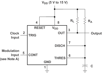
The operation of the timer can be modified by modulating the internal threshold and trigger voltages by applying an external voltage (or current) to CONT. Figure 7-3 shows a circuit for pulse-width modulation. A continuous input pulse train triggers the mono-stable circuit, and a control signal modulates the threshold voltage. Figure 7-4 shows the resulting output pulse-width modulation. While a sine-wave modulation signal is shown, any wave shape can be used.
GUID-CA6C90CE-D76D-4D49-8B25-FB013C7A3E57-low.gif
The modulating signal can be direct or capacitively coupled to CONT. For direct coupling, the effects of modulation source voltage and impedance on the bias of the timer must be considered.
Figure 7-3 Circuit for Pulse-Width Modulation