SLFS078C October 2006 – April 2024 TLC555-Q1
PRODUCTION DATA
- 1
- 1 Features
- 2 Applications
- 3 Description
- 4 Pin Configuration and Functions
- 5 Specifications
- 6 Detailed Description
- 7 Application and Implementation
- 8 Device and Documentation Support
- 9 Revision History
- 10Mechanical, Packaging, and Orderable Information
Package Options
Refer to the PDF data sheet for device specific package drawings
Mechanical Data (Package|Pins)
- D|8
Thermal pad, mechanical data (Package|Pins)
Orderable Information
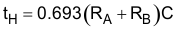
6.3.2 Astable Operation
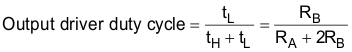
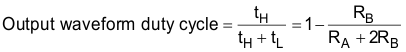
Figure 6-5 shows that adding a second resistor (RB) to the circuit and connecting the trigger input to the threshold input causes the timer to self-trigger and run as a multivibrator. The C capacitor charges through RA and RB and then only discharges through RB. As a result, the values of RA and RB control the duty cycle.
This astable connection results in the C capacitor charging and discharging between the threshold-voltage level (≈ 0.67 × VDD) and the trigger-voltage level (≈ 0.33 × VDD). As in the monostable circuit, charge and discharge times (and as a result, the frequency and duty cycle) are independent of the supply voltage.

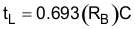
 Figure 6-6 Typical Astable Waveforms
 Figure 6-7 Trigger and Threshold Voltage Waveform
Figure 6-7 shows typical waveforms generated during astable operation. Calculate the output high-level duration (tH) and low-level duration tL for frequencies less than or equal to 100 kHz as follows:
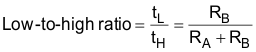
Other useful relationships are shown as follows:
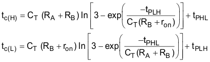
Equation 1 to Equation 7 do not account for any propagation delay times from the TRIG and THRES inputs to DISCH output. These delay times add directly to the period and overcharge the capacitor, which creates differences between calculated and actual values that increase with frequency. In addition, the internal on-state resistance ron during discharge adds to RB to provide another source of timing error in the calculation when RB is very low. The following equations provide better agreement with measured values. The formulas in Equation 8 represent the actual low and high times when used at higher frequencies (beyond 100 kHz) because propagation delay and discharge on resistance is added to the formulas. The value of CT includes both the nominal or deliberate timing capacitance, as well as parasitic capacitance on the PCB. Decoupling capacitance on CONT also affects the duty cycle, with an error contribution that depends on the capacitor leakage resistance. For additional discussion, see the Design low-duty-cycle timer circuits article.
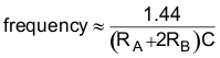
These equations and those given earlier are similar in that a time constant is multiplied by the logarithm of a number or function. The limit values of the logarithmic terms must be between ln(2) at low frequencies, and ln(3) at extremely high frequencies. For a duty cycle close to 50%, an appropriate constant for the logarithmic terms can be substituted with good results. Output waveform duty cycles less than 50% require that tc(H) / tc(L) < 1 and possibly that RA ≤ ron. These conditions can be difficult to obtain. Figure 6-8 shows the nominal free-running frequency associated with various combinations of CT and RA + 2 × RB.
 Figure 6-8 Free-Running Frequency