SLFS078C October 2006 – April 2024 TLC555-Q1
PRODUCTION DATA
- 1
- 1 Features
- 2 Applications
- 3 Description
- 4 Pin Configuration and Functions
- 5 Specifications
- 6 Detailed Description
- 7 Application and Implementation
- 8 Device and Documentation Support
- 9 Revision History
- 10Mechanical, Packaging, and Orderable Information
Package Options
Refer to the PDF data sheet for device specific package drawings
Mechanical Data (Package|Pins)
- D|8
Thermal pad, mechanical data (Package|Pins)
Orderable Information
6.3.1 Monostable Operation
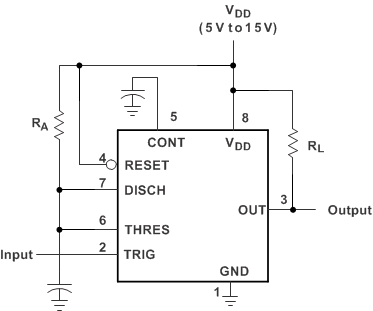
For monostable operation, Figure 6-2 shows how any of these timers can be connected. If the output is low, application of a negative-going pulse to the trigger (TRIG) sets the flip-flop (Q goes low), drives the output high, and turns off Q1. Capacitor C charges through RA until the voltage across the capacitor reaches the threshold voltage of the threshold (THRES) input. If TRIG returns to a high level, the output of the threshold comparator resets the flip-flop (Q goes high), drives the output low, and discharges C through Q1.
 Figure 6-2 Circuit for Monostable
Operation
Figure 6-2 Circuit for Monostable
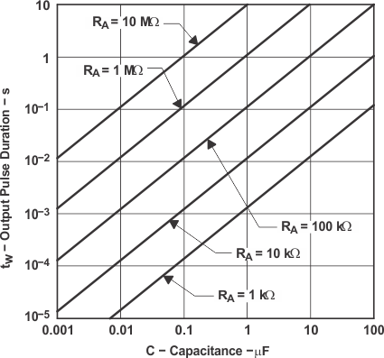
OperationMonostable operation is initiated when TRIG voltage falls below the trigger threshold. When initiated, the sequence ends only if TRIG is high for at least 10 µs before the end of the timing interval. When the trigger is grounded, the comparator storage time can be as long as 10 µs, which limits the minimum monostable pulse duration to 10 µs. Because of the threshold level and saturation voltage of Q1, the output pulse duration is approximately tw = 1.1RAC. Figure 6-3 is a plot of the time constant for various values of RA and C. The threshold levels and charge rates are directly proportional to the supply voltage (VDD). As a result, the timing interval is independent of the supply voltage if the supply voltage is constant during the time interval.
Applying a negative-going trigger pulse simultaneously to RESET and TRIG during the timing interval discharges C and reinitiates the cycle, commencing on the positive edge of the reset pulse. The output is held low as long as the reset pulse is low. To prevent false triggering, connect RESET to VDD when RESET is not being used. If the RESET function is required and the pin is driven by external logic or a microcontroller, use a pullup resistor to VDD (such as 10 kΩ) to prevent the RESET pin from floating. If the RESET function is not required, short the RESET pin directly to the VDD pin.
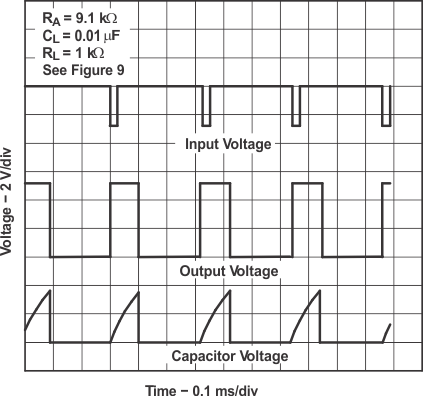
 Figure 6-3 Typical Monostable Waveforms
 Figure 6-4 Output Pulse Duration vs Capacitance