SGLS199C January   2004  â€“ July 2025 TLE2021-Q1 , TLE2021A-Q1 , TLE2022-Q1 , TLE2022A-Q1 , TLE2024-Q1

PRODUCTION DATA  

  1.   1
  2. 1Features
  3. 2Applications
  4. 3Description
  5. 4Pin Configuration and Functions
  6. 5Specifications
    1. 5.1  Absolute Maximum Ratings
    2. 5.2  Recommended Operating Conditions
    3. 5.3  Thermal Information for TLE2021-Q1
    4. 5.4  Thermal Information for TLE2022-Q1
    5. 5.5  Thermal Information for TLE2024-Q1
    6. 5.6  Electrical Characteristics for TLE2021-Q1, VCC = ±15V
    7. 5.7  Electrical Characteristics for TLE2021-Q1, VCC = 5V
    8. 5.8  Electrical Characteristics for TLE2022-Q1, VCC = ±15V
    9. 5.9  Electrical Characteristics for TLE2022-Q1, VCC = 5V
    10. 5.10 Electrical Characteristics for TLE2024-Q1, VCC = ±15V
    11. 5.11 Electrical Characteristics for TLE2024-Q1, VCC = 5V
    12. 5.12 Typical Characteristics
  7. 6Application and Implementation
    1. 6.1 Application Information
      1. 6.1.1 Voltage-Follower Applications
      2. 6.1.2 Input Offset Voltage Null
    2. 6.2 Layout
      1. 6.2.1 Layout Guidelines
      2. 6.2.2 Layout Example
  8. 7Device and Documentation Support
    1. 7.1 Receiving Notification of Documentation Updates
    2. 7.2 Support Resources
    3. 7.3 Trademarks
    4. 7.4 Electrostatic Discharge Caution
    5. 7.5 Glossary
  9. 8Revision History
  10. 9Mechanical, Packaging, and Orderable Information

Package Options

Refer to the PDF data sheet for device specific package drawings

Mechanical Data (Package|Pins)
  • D|8
Thermal pad, mechanical data (Package|Pins)
Orderable Information

Typical Characteristics

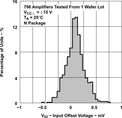
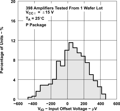
TLE2021-Q1 TLE2021A-Q1  TLE2022-Q1 TLE2022A-Q1  TLE2024-Q1 Distribution of TLE2021-Q1 Input Offset Voltage
 
Figure 5-1 Distribution of TLE2021-Q1 Input Offset Voltage
TLE2021-Q1 TLE2021A-Q1  TLE2022-Q1 TLE2022A-Q1  TLE2024-Q1 Distribution of TLE2024-Q1
                        Input Offset Voltage
 
Figure 5-3 Distribution of TLE2024-Q1 Input Offset Voltage
TLE2021-Q1 TLE2021A-Q1  TLE2022-Q1 TLE2022A-Q1  TLE2024-Q1 TLE2022-Q1 Input Bias Current
                        vs Common-Mode Input Voltage
 
Figure 5-5 TLE2022-Q1 Input Bias Current vs Common-Mode Input Voltage
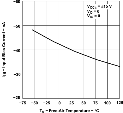
TLE2021-Q1 TLE2021A-Q1  TLE2022-Q1 TLE2022A-Q1  TLE2024-Q1 TLE2021-Q1 Input Bias Current vs Free-Air Temperature
Data at high and low temperatures applicable only within rated operating free-air temperature ranges of the various devices
Figure 5-7 TLE2021-Q1 Input Bias Current vs Free-Air Temperature
TLE2021-Q1 TLE2021A-Q1  TLE2022-Q1 TLE2022A-Q1  TLE2024-Q1 TLE2024-Q1 Input Bias Current vs Free-Air Temperature
Data at high and low temperatures applicable only within rated operating free-air temperature ranges of the various devices
Figure 5-9 TLE2024-Q1 Input Bias Current vs Free-Air Temperature
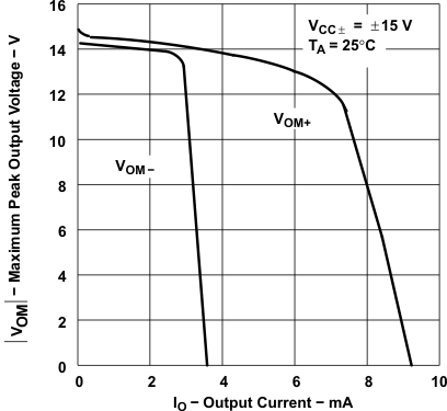
TLE2021-Q1 TLE2021A-Q1  TLE2022-Q1 TLE2022A-Q1  TLE2024-Q1 TLE2021-Q1 Maximum Peak Output Voltage vs Output Current
 
Figure 5-11 TLE2021-Q1 Maximum Peak Output Voltage vs Output Current
TLE2021-Q1 TLE2021A-Q1  TLE2022-Q1 TLE2022A-Q1  TLE2024-Q1 TLE2024-Q1 Maximum Peak
                        Output Voltage vs Output Current
 
 
Figure 5-13 TLE2024-Q1 Maximum Peak Output Voltage vs Output Current
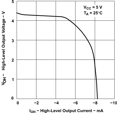
TLE2021-Q1 TLE2021A-Q1  TLE2022-Q1 TLE2022A-Q1  TLE2024-Q1 TLE2021-Q1 High-Level Output Voltage vs High-Level Output
                        Current
 
Figure 5-15 TLE2021-Q1 High-Level Output Voltage vs High-Level Output Current
TLE2021-Q1 TLE2021A-Q1  TLE2022-Q1 TLE2022A-Q1  TLE2024-Q1 High-Level Output Voltage
                        vs Free-Air Temperature
Data at high and low temperatures applicable only within rated operating free-air temperature ranges of the various devices
Figure 5-17 High-Level Output Voltage vs Free-Air Temperature
TLE2021-Q1 TLE2021A-Q1  TLE2022-Q1 TLE2022A-Q1  TLE2024-Q1 Low-Level Output Voltage
                        vs Free-Air Temperature
Data at high and low temperatures applicable only within rated operating free-air temperature ranges of the various devices
Figure 5-19 Low-Level Output Voltage vs Free-Air Temperature
TLE2021-Q1 TLE2021A-Q1  TLE2022-Q1 TLE2022A-Q1  TLE2024-Q1 Maximum Peak-to-Peak
                        Output Voltage vs Frequency
 
Figure 5-21 Maximum Peak-to-Peak Output Voltage vs Frequency
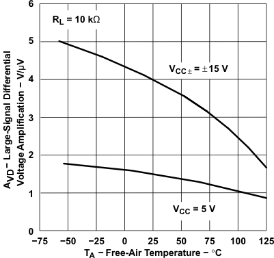
TLE2021-Q1 TLE2021A-Q1  TLE2022-Q1 TLE2022A-Q1  TLE2024-Q1 TLE2021-Q1 Large-Scale Differential Voltage Amplification vs
                        Free-Air Temperature
Data at high and low temperatures applicable only within rated operating free-air temperature ranges of the various devices
Figure 5-23 TLE2021-Q1 Large-Scale Differential Voltage Amplification vs Free-Air Temperature
TLE2021-Q1 TLE2021A-Q1  TLE2022-Q1 TLE2022A-Q1  TLE2024-Q1 TLE2024-Q1 Large-Scale
                        Differential Voltage Amplification vs Free-Air Temperature
Data at high and low temperatures applicable only within rated operating free-air temperature ranges of the various devices
Figure 5-25 TLE2024-Q1 Large-Scale Differential Voltage Amplification vs Free-Air Temperature
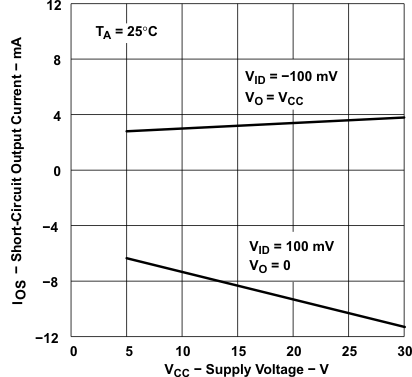
TLE2021-Q1 TLE2021A-Q1  TLE2022-Q1 TLE2022A-Q1  TLE2024-Q1 TLE2022-Q1 and TLE2024-Q1
                        Short-Circuit Output Current vs Supply Voltage
 
Figure 5-27 TLE2022-Q1 and TLE2024-Q1 Short-Circuit Output Current vs Supply Voltage
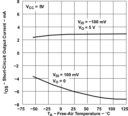
TLE2021-Q1 TLE2021A-Q1  TLE2022-Q1 TLE2022A-Q1  TLE2024-Q1 TLE2021-Q1 Short-Circuit Output Current vs Free-Air
                        Temperature
Data at high and low temperatures applicable only within rated operating free-air temperature ranges of the various devices
Figure 5-29 TLE2021-Q1 Short-Circuit Output Current vs Free-Air Temperature
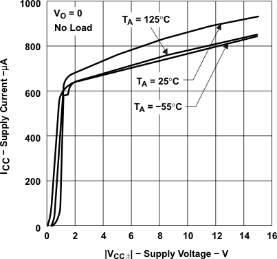
TLE2021-Q1 TLE2021A-Q1  TLE2022-Q1 TLE2022A-Q1  TLE2024-Q1 TLE2022-Q1 Supply Current vs
                        Supply Voltage
 
Figure 5-31 TLE2022-Q1 Supply Current vs Supply Voltage
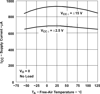
TLE2021-Q1 TLE2021A-Q1  TLE2022-Q1 TLE2022A-Q1  TLE2024-Q1 TLE2021-Q1 Supply Current vs Free-Air Temperature
Data at high and low temperatures applicable only within rated operating free-air temperature ranges of the various devices
Figure 5-33 TLE2021-Q1 Supply Current vs Free-Air Temperature
TLE2021-Q1 TLE2021A-Q1  TLE2022-Q1 TLE2022A-Q1  TLE2024-Q1 TLE2024-Q1 Supply Current vs
                        Free-Air Temperature
Data at high and low temperatures applicable only within rated operating free-air temperature ranges of the various devices
Figure 5-35 TLE2024-Q1 Supply Current vs Free-Air Temperature
TLE2021-Q1 TLE2021A-Q1  TLE2022-Q1 TLE2022A-Q1  TLE2024-Q1 TLE2022-Q1 Common-Mode
                        Rejection Ratio vs Frequency
 
Figure 5-37 TLE2022-Q1 Common-Mode Rejection Ratio vs Frequency
TLE2021-Q1 TLE2021A-Q1  TLE2022-Q1 TLE2022A-Q1  TLE2024-Q1 Voltage-Follower
                        Small-Signal Pulse Response
 
Figure 5-39 Voltage-Follower Small-Signal Pulse Response
TLE2021-Q1 TLE2021A-Q1  TLE2022-Q1 TLE2022A-Q1  TLE2024-Q1 TLE2021-Q1 Voltage-Follower Large-Signal Pulse Response
 
Figure 5-41 TLE2021-Q1 Voltage-Follower Large-Signal Pulse Response
TLE2021-Q1 TLE2021A-Q1  TLE2022-Q1 TLE2022A-Q1  TLE2024-Q1 TLE2024-Q1 Voltage-Follower Large-Scale Pulse Response
 
Figure 5-43 TLE2024-Q1 Voltage-Follower Large-Scale Pulse Response
TLE2021-Q1 TLE2021A-Q1  TLE2022-Q1 TLE2022A-Q1  TLE2024-Q1 TLE2022-Q1 Voltage-Follower Large-Signal Pulse Response
 
Figure 5-45 TLE2022-Q1 Voltage-Follower Large-Signal Pulse Response
TLE2021-Q1 TLE2021A-Q1  TLE2022-Q1 TLE2022A-Q1  TLE2024-Q1 Peak-to-Peak Equivalent
                        Input Noise Voltage 0.1Hz to 1Hz
 
Figure 5-47 Peak-to-Peak Equivalent Input Noise Voltage 0.1Hz to 1Hz
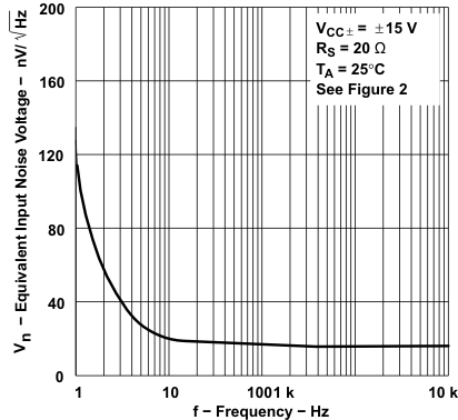
TLE2021-Q1 TLE2021A-Q1  TLE2022-Q1 TLE2022A-Q1  TLE2024-Q1 Equivalent Input Noise
                        Voltage vs Frequency
 
Figure 5-49 Equivalent Input Noise Voltage vs Frequency
TLE2021-Q1 TLE2021A-Q1  TLE2022-Q1 TLE2022A-Q1  TLE2024-Q1 TLE2022-Q1 and TLE2024-Q1 Unity-Gain
                        Bandwidth vs Supply Voltage
 
Figure 5-51 TLE2022-Q1 and TLE2024-Q1 Unity-Gain Bandwidth vs Supply Voltage
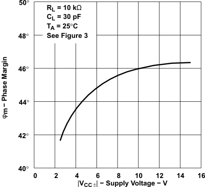
TLE2021-Q1 TLE2021A-Q1  TLE2022-Q1 TLE2022A-Q1  TLE2024-Q1 TLE2022-Q1 and TLE2024-Q1 Phase Margin
                        vs Supply Voltage
 
Figure 5-53 TLE2022-Q1 and TLE2024-Q1 Phase Margin vs Supply Voltage
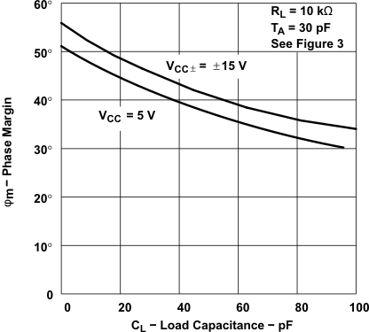
TLE2021-Q1 TLE2021A-Q1  TLE2022-Q1 TLE2022A-Q1  TLE2024-Q1 TLE2022-Q1 and TLE2024-Q1 Phase Margin
                        vs Load Capacitance
 
Figure 5-55 TLE2022-Q1 and TLE2024-Q1 Phase Margin vs Load Capacitance
TLE2021-Q1 TLE2021A-Q1  TLE2022-Q1 TLE2022A-Q1  TLE2024-Q1 Distribution of TLE2022-Q1
                        Input Offset Voltage
 
Figure 5-2 Distribution of TLE2022-Q1 Input Offset Voltage
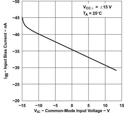
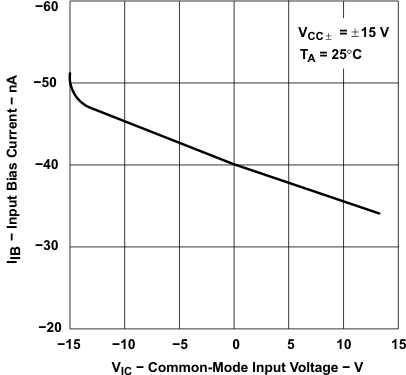
TLE2021-Q1 TLE2021A-Q1  TLE2022-Q1 TLE2022A-Q1  TLE2024-Q1 TLE2021-Q1 Input Bias Current vs Common-Mode Input Voltage
 
Figure 5-4 TLE2021-Q1 Input Bias Current vs Common-Mode Input Voltage
TLE2021-Q1 TLE2021A-Q1  TLE2022-Q1 TLE2022A-Q1  TLE2024-Q1 TLE2024-Q1 Input Bias Current
                        vs Common-Mode Input Voltage
 
Figure 5-6 TLE2024-Q1 Input Bias Current vs Common-Mode Input Voltage
TLE2021-Q1 TLE2021A-Q1  TLE2022-Q1 TLE2022A-Q1  TLE2024-Q1 TLE2022-Q1 Input Bias Current vs Free-Air Temperature
Data at high and low temperatures applicable only within rated operating free-air temperature ranges of the various devices
Figure 5-8 TLE2022-Q1 Input Bias Current vs Free-Air Temperature
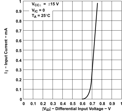
TLE2021-Q1 TLE2021A-Q1  TLE2022-Q1 TLE2022A-Q1  TLE2024-Q1 Input Current vs
                        Differential Input Voltage
 
 
Figure 5-10 Input Current vs Differential Input Voltage
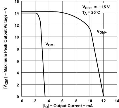
TLE2021-Q1 TLE2021A-Q1  TLE2022-Q1 TLE2022A-Q1  TLE2024-Q1 TLE2022-Q1 Maximum Peak Output Voltage vs Output Current
 
Figure 5-12 TLE2022-Q1 Maximum Peak Output Voltage vs Output Current
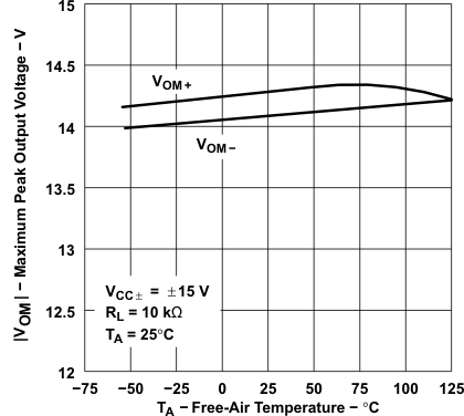
TLE2021-Q1 TLE2021A-Q1  TLE2022-Q1 TLE2022A-Q1  TLE2024-Q1 Maximum Peak Output
                        Voltage vs Free-Air Temperature
Data at high and low temperatures applicable only within rated operating free-air temperature ranges of the various devices
Figure 5-14 Maximum Peak Output Voltage vs Free-Air Temperature
TLE2021-Q1 TLE2021A-Q1  TLE2022-Q1 TLE2022A-Q1  TLE2024-Q1 TLE2022-Q1 and TLE2024-Q1
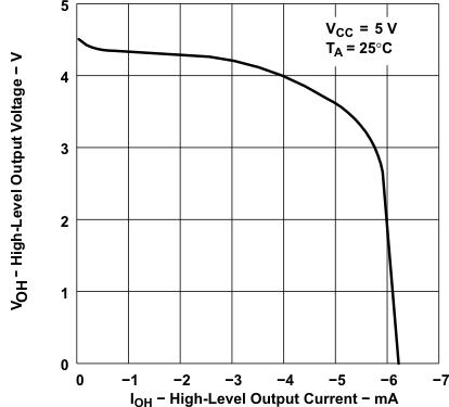
                        High-Level Output Voltage vs High-Level Output Current
 
Figure 5-16 TLE2022-Q1 and TLE2024-Q1 High-Level Output Voltage vs High-Level Output Current
TLE2021-Q1 TLE2021A-Q1  TLE2022-Q1 TLE2022A-Q1  TLE2024-Q1 Low-Level Output Voltage
                        vs Low-Level Output Current
 
 
Figure 5-18 Low-Level Output Voltage vs Low-Level Output Current
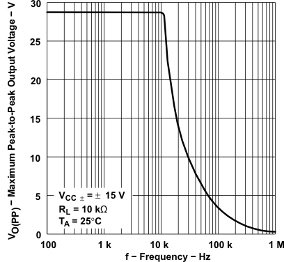
TLE2021-Q1 TLE2021A-Q1  TLE2022-Q1 TLE2022A-Q1  TLE2024-Q1 Maximum Peak-to-Peak
                        Output Voltage Vs Frequency
 
 
Figure 5-20 Maximum Peak-to-Peak Output Voltage Vs Frequency
TLE2021-Q1 TLE2021A-Q1  TLE2022-Q1 TLE2022A-Q1  TLE2024-Q1 Large-Signal Differential
                        Voltage Amplification and Phase Shift vs Frequency
 
Figure 5-22 Large-Signal Differential Voltage Amplification and Phase Shift vs Frequency
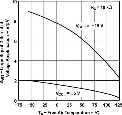
TLE2021-Q1 TLE2021A-Q1  TLE2022-Q1 TLE2022A-Q1  TLE2024-Q1 TLE2022-Q1 Large-Signal
                        Differential Voltage Amplification vs Free-Air Temperature
Data at high and low temperatures applicable only within rated operating free-air temperature ranges of the various devices
Figure 5-24 TLE2022-Q1 Large-Signal Differential Voltage Amplification vs Free-Air Temperature
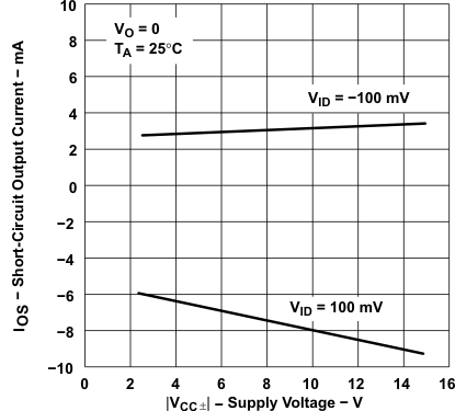
TLE2021-Q1 TLE2021A-Q1  TLE2022-Q1 TLE2022A-Q1  TLE2024-Q1 TLE2021-Q1 Short-Circuit Output Current vs Supply Voltage
 
 
Figure 5-26 TLE2021-Q1 Short-Circuit Output Current vs Supply Voltage
TLE2021-Q1 TLE2021A-Q1  TLE2022-Q1 TLE2022A-Q1  TLE2024-Q1 TLE2021-Q1 Short-Circuit Output Current vs Supply Voltage
 
Figure 5-28 TLE2021-Q1 Short-Circuit Output Current vs Supply Voltage
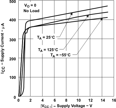
TLE2021-Q1 TLE2021A-Q1  TLE2022-Q1 TLE2022A-Q1  TLE2024-Q1 TLE2021-Q1 Supply Current vs Supply Voltage
 
 
Figure 5-30 TLE2021-Q1 Supply Current vs Supply Voltage
TLE2021-Q1 TLE2021A-Q1  TLE2022-Q1 TLE2022A-Q1  TLE2024-Q1 TLE2024-Q1 Supply Current vs
                        Supply Voltage
 
Figure 5-32 TLE2024-Q1 Supply Current vs Supply Voltage
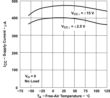
TLE2021-Q1 TLE2021A-Q1  TLE2022-Q1 TLE2022A-Q1  TLE2024-Q1 TLE2022-Q1 Supply Current vs
                        Free-Air Temperature
Data at high and low temperatures applicable only within rated operating free-air temperature ranges of the various devices
Figure 5-34 TLE2022-Q1 Supply Current vs Free-Air Temperature
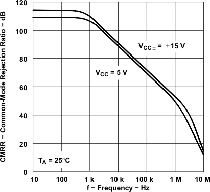
TLE2021-Q1 TLE2021A-Q1  TLE2022-Q1 TLE2022A-Q1  TLE2024-Q1 TLE2021-Q1 Common-Mode Rejection Ratio vs Frequency
 
 
Figure 5-36 TLE2021-Q1 Common-Mode Rejection Ratio vs Frequency
TLE2021-Q1 TLE2021A-Q1  TLE2022-Q1 TLE2022A-Q1  TLE2024-Q1 TLE2024-Q1 Common-Mode
                        Rejection Ratio vs Frequency
 
Figure 5-38 TLE2024-Q1 Common-Mode Rejection Ratio vs Frequency
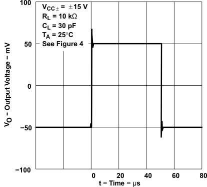
TLE2021-Q1 TLE2021A-Q1  TLE2022-Q1 TLE2022A-Q1  TLE2024-Q1 Voltage-Follower
                        Small-Signal Pulse Response
 
Figure 5-40 Voltage-Follower Small-Signal Pulse Response
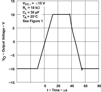
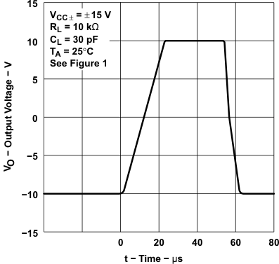
TLE2021-Q1 TLE2021A-Q1  TLE2022-Q1 TLE2022A-Q1  TLE2024-Q1 TLE2022-Q1 Voltage-Follower Large-Signal Pulse Response
 
Figure 5-42 TLE2022-Q1 Voltage-Follower Large-Signal Pulse Response
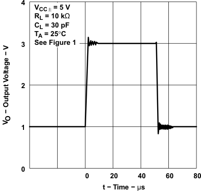
TLE2021-Q1 TLE2021A-Q1  TLE2022-Q1 TLE2022A-Q1  TLE2024-Q1 TLE2021-Q1 Voltage-Follower Large-Signal Pulse Response
 
Figure 5-44 TLE2021-Q1 Voltage-Follower Large-Signal Pulse Response
TLE2021-Q1 TLE2021A-Q1  TLE2022-Q1 TLE2022A-Q1  TLE2024-Q1 TLE2024-Q1 Voltage-Follower Large-Signal Pulse Response
 
Figure 5-46 TLE2024-Q1 Voltage-Follower Large-Signal Pulse Response
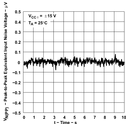
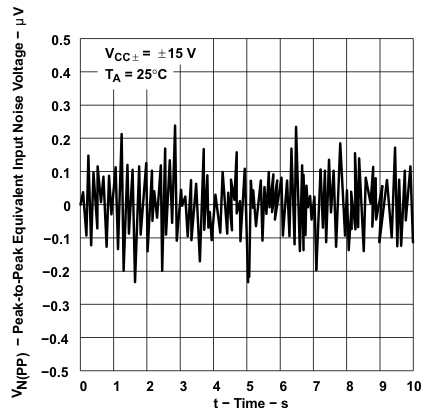
TLE2021-Q1 TLE2021A-Q1  TLE2022-Q1 TLE2022A-Q1  TLE2024-Q1 Peak-to-Peak Equivalent
                        Input Noise Voltage 0.1Hz to 10Hz
 
Figure 5-48 Peak-to-Peak Equivalent Input Noise Voltage 0.1Hz to 10Hz
TLE2021-Q1 TLE2021A-Q1  TLE2022-Q1 TLE2022A-Q1  TLE2024-Q1 TLE2021-Q1 Unity-Gain Bandwidth vs Supply Voltage
 
Figure 5-50 TLE2021-Q1 Unity-Gain Bandwidth vs Supply Voltage
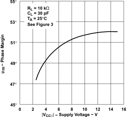
TLE2021-Q1 TLE2021A-Q1  TLE2022-Q1 TLE2022A-Q1  TLE2024-Q1 TLE2021-Q1 Phase Margin vs Supply Voltage
 
Figure 5-52 TLE2021-Q1 Phase Margin vs Supply Voltage
TLE2021-Q1 TLE2021A-Q1  TLE2022-Q1 TLE2022A-Q1  TLE2024-Q1 TLE2021-Q1 Phase Margin vs Load Capacitance
 
Figure 5-54 TLE2021-Q1 Phase Margin vs Load Capacitance