SLLSEC7A August 2012 – October 2015 TLK10034
PRODUCTION DATA.
- 1Device Overview
- 2Revision History
- 3Pin Configuration and Functions
-
4Specifications
- 4.1 Absolute Maximum Ratings
- 4.2 ESD Ratings
- 4.3 Recommended Operating Conditions
- 4.4 Thermal Information
- 4.5 LVCMOS Electrical Characteristics (VDDO)
- 4.6 High Speed Side Serial Transmitter Characteristics
- 4.7 High Speed Side Serial Receiver Characteristics
- 4.8 Low Speed Side Serial Transmitter Characteristics
- 4.9 Low Speed Side Serial Receiver Characteristics
- 4.10 Reference Clock Characteristics (REFCLK0P/N, REFCLK1P/N)
- 4.11 Differential Output Clock Characteristics (CLKOUTA/B/C/DP/N)
- 4.12 MDIO Timing Requirements
- 4.13 JTAG Timing Requirements
- 4.14 Typical Characteristics
-
5Detailed Description
- 5.1 Overview
- 5.2 Functional Block Diagrams
- 5.3
Feature Description
- 5.3.1
10GBASE-KR Mode
- 5.3.1.1 10GBASE-KR Transmit Data Path Overview
- 5.3.1.2 10GBASE-KR Receive Data Path Overview
- 5.3.1.3 Channel Synchronization Block
- 5.3.1.4 8B/10B Encoder
- 5.3.1.5 8B/10B Decoder
- 5.3.1.6 64B/66B Encoder/Scrambler
- 5.3.1.7 64B/66B Decoder/Descrambler
- 5.3.1.8 Transmit Gearbox
- 5.3.1.9 Receive Gearbox
- 5.3.1.10 XAUI Lane Alignment / Code Gen (XAUI PCS)
- 5.3.1.11 XAUI Inter-Packet Gap (IPG) Handling
- 5.3.1.12 Clock Tolerance Compensation (CTC)
- 5.3.1.13 10GBASE-KR Auto-Negotiation
- 5.3.1.14 10GBASE-KR Link Training
- 5.3.1.15 Forward Error Correction
- 5.3.1.16 10GBASE-KR Line Rate, PLL Settings, and Reference Clock Selection
- 5.3.1.17 10GBASE-KR Loopback Modes
- 5.3.1.18 10GBASE-KR Test Pattern Support
- 5.3.1.19 10GBASE-KR Latency
- 5.3.2 1GBASE-KX Mode
- 5.3.3
General Purpose (10G) SerDes Mode
- 5.3.3.1 General Purpose SERDES Transmit Data Path
- 5.3.3.2 General Purpose SERDES Receive Data Path
- 5.3.3.3 Channel Synchronization
- 5.3.3.4 8B/10B Encoder and Decoder
- 5.3.3.5 Lane Alignment Scheme for 8b/10b General Purpose Serdes Mode (Non XAUI Fata, - No /A/)
- 5.3.3.6 Lane Alignment Components
- 5.3.3.7 Lane Alignment Operation (General Purpose Serdes Mode)
- 5.3.3.8 Line Rate, SERDES PLL Settings, and Reference Clock Selection for the General Purpose SERDES Mode
- 5.3.3.9 General Purpose (10G) Loopback Modes
- 5.3.3.10 General Purpose (10G) Latency Measurement Function
- 5.3.3.11 General Purpose (10G) Mode Latency
- 5.3.3.12 TLK10034 Clocks: REFCLK, CLKOUT
- 5.3.3.13 TLK10034 Control Pins and Interfaces
- 5.3.3.14 MDIO Interface
- 5.3.3.15 JTAG Interface
- 5.3.3.16 Unused Pins
- 5.3.4 Provisionable XAUI Clock Tolerance Compensation
- 5.3.1
10GBASE-KR Mode
- 5.4 Device Functional Modes
- 5.5 Memory
- 5.6 Register Map
- 6Application and Implementation
- 7Device and Documentation Support
- 8Mechanical, Packaging, and Orderable Information
Package Options
Mechanical Data (Package|Pins)
- AAJ|324
Thermal pad, mechanical data (Package|Pins)
Orderable Information
4 Specifications
4.1 Absolute Maximum Ratings
over operating free-air temperature range (unless otherwise noted)(1)| MIN | MAX | UNIT | ||
|---|---|---|---|---|
| Supply voltage | DVDD, VDDA, LS/HS, VPP, VDDD | –0.3 | 1.4 | V |
| VDDRA/B/C/D_LS/HS, VDDO[3:0] | –0.3 | 2.2 | V | |
| Input Voltage, VI | LVCMOS/CML/Analog | –0.3 | Supply + 0.3 | V |
| Characterized free-air operating temerature | –40 | 85 | °C | |
| Storage temperature Tstg | –65 | 85 | °C | |
(1) Stresses beyond those listed under Absolute Maximum Ratings may cause permanent damage to the device. These are stress ratings only, which do not imply functional operation of the device at these or any other conditions beyond those indicated under Recommended Operating Conditions. Exposure to absolute-maximum-rated conditions for extended periods may affect device reliability.
4.2 ESD Ratings
| VALUE | UNIT | |||
|---|---|---|---|---|
| V(ESD) | Electrostatic discharge | Human-body model (HBM), per ANSI/ESDA/JEDEC JS-001(1) | ±1500 | V |
| Charged-device model (CDM), per JEDEC specification JESD22-C101(2) | ±500 | |||
(1) JEDEC document JEP155 states that 500-V HBM allows safe manufacturing with a standard ESD control process.
(2) JEDEC document JEP157 states that 250-V CDM allows safe manufacturing with a standard ESD control process
4.3 Recommended Operating Conditions
over operating free-air temperature range (unless otherwise noted)| MIN | NOM | MAX | UNIT | ||||
|---|---|---|---|---|---|---|---|
| Digital / analog supply voltages | VDDD, VDDA_LS/HS, DVDD, VDDT_LS/HS, VPP | 0.95 | 1.00 | 1.05 | V | ||
| SERDES PLL regulator voltage | VDDRA_LS/HS, VDDRB_LS/HS, VDDRC_LS/HS, VDDRD_LS/HS | 1.5-V Nominal | 1.425 | 1.5 | 1.575 | V | |
| 1.8-V Nominal | 1.71 | 1.8 | 1.89 | ||||
| LVCMOS I/O supply voltage | VDDO[3:0] | 1.5-V Nominal | 1.425 | 1.5 | 1.575 | V | |
| 1.8-V Nominal | 1.71 | 1.8 | 1.89 | ||||
| IDD | Supply current | VDDD | 10.3 Gbps | 913 | mA | ||
| VDDA_LS/HS | 1020 | ||||||
| DVDD + VPP | 1117 | ||||||
| VDDT_LS/HS | 1249 | ||||||
| VDDRA/B/C/D_LS | 168 | ||||||
| VDDRA/B/C/D_HS | 118 | ||||||
| VDDO[3:0] | 10 | ||||||
| PD | Power dissipation | Nominal | 3.3 | W | |||
| All supplies worst case, 10GBASE-KR |
3.7(1) | ||||||
| ISD | Shutdown current | VDDD | PD* Asserted | 125 | mA | ||
| VDDA | 60 | ||||||
| DVDD + VPP | 130 | ||||||
| VDDT | 95 | ||||||
| VDDRA_HS/LS + VDDRB_HS/LS + VDDRC_HS/LS + VDDRD_HS/LS | 5 | ||||||
| VDDO | 10 | ||||||
(1) Total worst-case power is not a sum of the individual power supply worst cases, as the individual worst-case powers are taken from multiple modes. These modes are mutually exclusive and therefore used only for power supply requirements.
4.4 Thermal Information
| THERMAL METRIC(1) | TLK10034 | UNIT | |
|---|---|---|---|
| AAJ (FCBGA) | |||
| 324 PINS | |||
| RθJA | Junction-to-ambient thermal resistance | 21.2 | °C/W |
| RθJC(top) | Junction-to-case (top) thermal resistance | 0.2 | °C/W |
| RθJB | Junction-to-board thermal resistance | 7.9 | °C/W |
| ψJT | Junction-to-top characterization parameter | 0.1 | °C/W |
| ψJB | Junction-to-board characterization parameter | 7.7 | °C/W |
| RθJC(bot) | Junction-to-case (bottom) thermal resistance | n/a | °C/W |
(1) For more information about traditional and new thermal metrics, see the Semiconductor and IC Package Thermal Metrics application report, SPRA953.
4.5 LVCMOS Electrical Characteristics (VDDO)
| PARAMETER | TEST CONDITIONS | MIN | TYP | MAX | UNIT | |
|---|---|---|---|---|---|---|
| VOH | High-level output voltage | IOH = 2 mA, Driver Enabled (1.8V) | VDDO – 0.45 | VDDO | V | |
| IOH = 2 mA, Driver Enabled (1.5V) | 0.75 × VDDO | |||||
| VOL | Low-level output voltage | IOL = –2 mA, Driver Enabled (1.8V) | 0 | 0.45 | V | |
| IOL = –2 mA, Driver Enabled (1.5V) | 0.25 × VDDO | |||||
| VIH | High-level input voltage | 0.65 × VDDO | VDDO + 0.3 | V | ||
| VIL | Low-level input voltage | –0.3 | 0.35 × VDDO | V | ||
| IIH, IIL | Receiver only | Low/High Input Current | ±170 | µA | ||
| IOZ | Driver only | Driver Disabled | ±25 | µA | ||
| Driver/Receiver With Pullup/Pulldown | Driver disabled With Pull Up/Down Enabled | ±195 | ||||
| CIN | Input capacitance | 3 | pF | |||
4.6 High Speed Side Serial Transmitter Characteristics
| PARAMETER | TEST CONDITIONS | MIN | TYP | MAX | UNIT | |
|---|---|---|---|---|---|---|
| VOD(p-p) | TX Output differential peak-to-peak voltage swing, transmitter enabled | SWING (3.15:22) = 0000 | 50 | 130 | 220 | mVpp |
| SWING (3.15:22) = 0001 | 110 | 220 | 320 | |||
| SWING (3.15:22) = 0010 | 180 | 300 | 430 | |||
| SWING (3.15:22) = 0011 | 250 | 390 | 540 | |||
| SWING (3.15:22) = 0100 | 320 | 480 | 650 | |||
| SWING (3.15:22) = 0101 | 390 | 570 | 770 | |||
| SWING (3.15:22) = 0110 | 460 | 660 | 880 | |||
| SWING (3.15:22) = 0111 | 530 | 750 | 1000 | |||
| SWING (3.15:22) = 1000 | 590 | 830 | 1100 | |||
| SWING (3.15:22) = 1001 | 660 | 930 | 1220 | |||
| SWING (3.15:22) = 1010 | 740 | 1020 | 1320 | |||
| SWING (3.15:22) = 1011 | 820 | 1110 | 1430 | |||
| SWING (3.15:22) = 1100 | 890 | 1180 | 1520 | |||
| SWING (3.15:22) = 1101 | 970 | 1270 | 1610 | |||
| SWING (3.15:22) = 1110 | 1060 | 1340 | 1680 | |||
| SWING (3.15:22) = 1111 | 1090 | 1400 | 1740 | |||
| Transmitter disabled | 30 | |||||
| Vpre/post | TX Output pre/post cursor emphasis voltage | See register bits TWPOST1, TWPOST2, and TWPRE for de-emphasis settings. See Figure 4-2 |
–17.5/ –37.5% |
+17.5/ +37.5% |
||
| VCMT | TX Output common mode voltage | 100-Ω differential termination. DC-coupled. | VDDT - .25*VOD(p-p) | mV | ||
| tskew | Intra-pair output skew | Serial Rate = 9.8304 Gbps | 0.045 | UI | ||
| Tr, Tf | Differential output signal rise, fall time (20% to 80%), Differential Load = 100Ω |
24 | ps | |||
| JT1 | Serial output total jitter (CPRI LV/LV-II/LV-III, OBSAI and 10GBASE-KR Rates) | Serial Rate ≤ 3.072Gbps | 0.35 | UIpp | ||
| Serial Rate > 3.072Gbps | 0.28 | |||||
| JD1 | Serial output deterministic jitter (CPRI LV/LV-II, OBSAI and 10GBASE-KR Rates) | Serial Rate ≤ 3.072Gbps | 0.17 | UIpp | ||
| Serial Rate > 3.072Gbps | 0.15 | |||||
| JR1 | Serial output random jitter (CPRI LV/LV-II/LV-III, OBSAI and 10GBASE-KR Rates) | Serial Rate > 3.072Gbps | 0.15 | UIpp | ||
| JT2 | Serial output total jitter (CPRI E.6/12.HV) | Serial Rate = 0.6144 and 1.2288Gbps | 0.279 | UIpp | ||
| JD2 | Serial output deterministic jitter (CPRI E.6/12.HV) | 0.14 | ||||
| SDD22 | Differential output return loss | 50 MHz < f < 2.5 GHz | 9 | dB | ||
| 2.5 GHz < f < 7.5 GHz | See (1) | dB | ||||
| SCC22 | Common-mode output return loss | 50 MHz < f < 2.5 GHz | 6 | dB | ||
| 2.5 GHz < f < 7.5 GHz | See (2) | dB | ||||
| T(LATENCY) | Transmit path latency | 10GBASE-KR mode | see Figure 5-10 | |||
| 1GBASE-KX mode | see Figure 5-11 | |||||
| General Purpose mode | see Figure 5-18 | |||||
(1) Differential input return loss, SDD22 = 9 – 12 log10(f / 2500MHz)) dB
(2) Common-mode output return loss, SDD22 = 6 – 12 log10(f / 2500MHz)) dB
4.7 High Speed Side Serial Receiver Characteristics
| PARAMETER | TEST CONDITIONS | MIN | TYP | MAX | UNIT | |
|---|---|---|---|---|---|---|
| VID | RX Input differential voltage, |RXP – RXN| | Full Rate, AC Coupled | 50 | 600 | mV | |
| Half/Quarter/Eighth Rate, AC Coupled | 50 | 800 | ||||
| VID(pp) | RX Input differential peak-to-peak voltage swing, 2×|RXP – RXN| | Full Rate, AC Coupled | 100 | 1200 | mVpp | |
| Half/Quarter/Eighth Rate, AC Coupled | 100 | 1600 | ||||
| CI | RX Input capacitance | 2 | pF | |||
| JTOL | 10GBASE-KR Jitter tolerance, test channel with mTC =1 (see Figure 4-5 for attenuation curve), PRBS31 test pattern at 10.3125 Gbps | Applied sinusoidal jitter | 0.115 | UIpp | ||
| Applie drandom jitter | 0.130 | |||||
| Applied duty cycle distortion | 0.035 | |||||
| Broadband noise amplitude (RMS) | 5.2 | |||||
| SDD11 | Differential input return loss | 50 MHz < f < 2.5 GHz | 9 | dB | ||
| 2.5 GHz < f < 7.5 GHz | See (1) | |||||
| tskew | Intra-pair input skew | 0.23 | UI | |||
| t(LATENCY) | Receive path latency | 10GBASE-KR mode | see Figure 5-10 | |||
| 1GBASE-KX mode | see Figure 5-11 | |||||
| General Purpose mode | see Figure 5-18 | |||||
(1) Differential input return loss, SDD11 = 9 – 12 log10(f / 2.5GHz)) dB
4.8 Low Speed Side Serial Transmitter Characteristics
| PARAMETER | TEST CONDITIONS | MIN | TYP | MAX | UNIT | |
|---|---|---|---|---|---|---|
| VOD(pp) | Transmitter output differential peak-to-peak voltage swing | SWING = 000 | 110 | 190 | 280 | mVpp |
| SWING = 001 | 280 | 380 | 490 | |||
| SWING = 010 | 420 | 560 | 700 | |||
| SWING = 011 | 560 | 710 | 870 | |||
| SWING = 100 | 690 | 850 | 1020 | |||
| SWING = 101 | 760 | 950 | 1150 | |||
| SWING = 110 | 800 | 1010 | 1230 | |||
| SWING = 111 | 830 | 1050 | 1270 | |||
| DE | Transmitter output de-emphasis voltage swing reduction | DE = 0000 | 0 | dB | ||
| DE = 0001 | 0.42 | |||||
| DE = 0010 | 0.87 | |||||
| DE = 0011 | 1.34 | |||||
| DE = 0100 | 1.83 | |||||
| DE = 0101 | 2.36 | |||||
| DE = 0110 | 2.92 | |||||
| DE = 0111 | 3.52 | |||||
| DE = 1000 | 4.16 | |||||
| DE = 1001 | 4.86 | |||||
| DE = 1010 | 5.61 | |||||
| DE = 1011 | 6.44 | |||||
| DE = 1100 | 7.35 | |||||
| DE = 1101 | 8.38 | |||||
| DE = 1110 | 9.54 | |||||
| DE = 1111 | 10.87 | |||||
| VCMT | Transmitter output common mode voltage | 100-Ω differential termination. DC-coupled. | VDDT-.5*VDD(p-p) | mV | ||
| tskew | Intra-pair output skew | 0.045 | UI | |||
| tR, tF | Differential output signal rise, fall time (20% to 80%) Differential Load = 100Ω | 30 | ps | |||
| JT | Serial output total jitter | 0.35 | UI | |||
| JD | Serial output deterministic jitter | 0.17 | UI | |||
| tskew | Lane-to-lane output skew | 50 | ps | |||
4.9 Low Speed Side Serial Receiver Characteristics
| PARAMETER | TEST CONDITIONS | MIN | TYP | MAX | UNIT | |
|---|---|---|---|---|---|---|
| VID | Receiver input differential voltage, |INP – INN| | Full Rate, AC Coupled | 50 | 600 | mV | |
| Half/Quarter Rate, AC Coupled | 50 | 800 | ||||
| VID(pp) | Receiver input differential peak-to-peak voltage swing 2×|INP – INN| | Full Rate, AC Coupled | 100 | 1200 | mVdfpp | |
| Half/Quarter Rate, AC Coupled | 100 | 1600 | ||||
| CI | Receiver input capacitance | 2 | pF | |||
| JTOL | Jitter tolerance, total jitter at serial input (DJ + RJ) (BER 10-15) | Zero crossing, Half/Quarter Rate | 0.66 | UIp-p | ||
| Zero crossing, Full Rate | 0.65 | |||||
| JDR | Serial input deterministic jitter (BER 10-15) | Zero crossing, Half/Quarter Rate | 0.50 | UIp-p | ||
| Zero crossing, Full Rate | 0.35 | |||||
| tskew | Intra-pair input skew | 0.23 | UI | |||
| tlane-skew | Lane-to-lane input skew | 30 | UI | |||
4.10 Reference Clock Characteristics (REFCLK0P/N, REFCLK1P/N)
| PARAMETER | TEST CONDITIONS | MIN | TYP | MAX | UNIT | |
|---|---|---|---|---|---|---|
| F | Frequency | 122.88 | 425 | MHz | ||
| FHSoffset | Accuracy | Relative to Nominal HS Serial Data Rate | –100 | 100 | ppm | |
| Relative to Incoming HS Serial Data Rate | –200 | 200 | ||||
| DC | Duty cycle | High Time | 45% | 50% | 55% | |
| VID | Differential input voltage | 250 | 2000 | mVpp | ||
| CIN | Input capacitance | 1 | pF | |||
| RIN | Differential input impedance | 80 | 100 | 120 | Ω | |
| TRISE | Rise/fall time | 10% to 90% | 50 | 350 | ps | |
| JR | Random jitter | 10 kHz to 1 MHz | 3 | ps-RMS | ||
| Above 1 MHz | 1 | ps-RMS | ||||
4.11 Differential Output Clock Characteristics (CLKOUTA/B/C/DP/N)
| PARAMETER | TEST CONDITIONS | MIN | TYP | MAX | UNIT | |
|---|---|---|---|---|---|---|
| VOD | Differential output voltage | Peak to peak | 1000 | 2000 | mVpp | |
| TRISE | Output rise time | 10% to 90%, 2pF lumped capacitive load, AC-Coupled | 350 | ps | ||
| RTERM | Output termination | CLKOUT×P/N to DVDD | 50 | Ω | ||
| F | Output frequency | 0 | 500 | MHz | ||
4.12 MDIO Timing Requirements
over recommended operating conditions (unless otherwise noted)| MIN | NOM | MAX | UNIT | |||
|---|---|---|---|---|---|---|
| tperiod | MDC period | See Figure 4-3 | 100 | ns | ||
| tsetup | MDIO setup to ↑ MDC | 10 | ns | |||
| thold | MDIO hold to ↑ MDC | 10 | ns | |||
| Tvalid | MDIO valid from MDC ↑ | 0 | 40 | ns | ||
4.13 JTAG Timing Requirements
over recommended operating conditions (unless otherwise noted)| MIN | NOM | MAX | UNIT | |||
|---|---|---|---|---|---|---|
| TPERIOD | TCK period | See Figure 4-4 | 66.67 | ns | ||
| TSETUP | TDI/TMS/TRST_N setup to ↑ TCK | 3 | ||||
| THOLD | TDI/TMS/TRST_N hold from ↑ TCK | 5 | ||||
| TVALID | TDO delay from TCK Falling | 0 | 10 | ns | ||
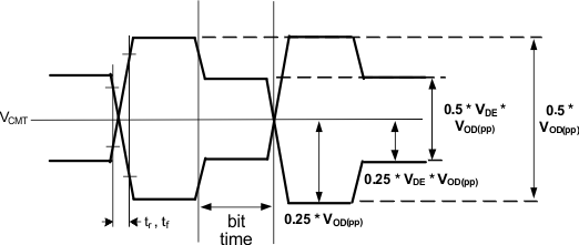 Figure 4-1 Transmit Output Waveform Parameter Definitions
 Figure 4-2 Pre and Post Cursor Swing Definitions
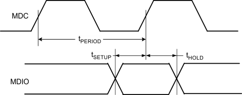 Figure 4-3 MDIO Read and Write Timing
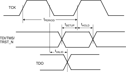 Figure 4-4 JTAG Timing
4.14 Typical Characteristics
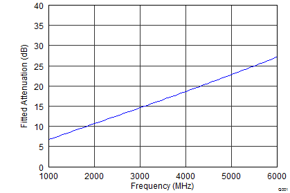
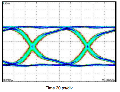 Figure 4-6 Eye Diagram of the TLK100034 at 10.3125 Gbps Under Nominal Conditions