SBOS884A October 2017 – December 2018 TLV2313-Q1 , TLV313-Q1
PRODUCTION DATA.
- 1 Features
- 2 Applications
- 3 Description
- 4 Revision History
- 5 Device Comparison Table
- 6 Pin Configuration and Functions
-
7 Specifications
- 7.1 Absolute Maximum Ratings
- 7.2 ESD Ratings
- 7.3 Recommended Operating Conditions
- 7.4 Thermal Information: TLV313-Q1
- 7.5 Thermal Information: TLV2313-Q1
- 7.6 Electrical Characteristics: 5.5 V
- 7.7 Electrical Characteristics: 1.8 V
- 7.8 Typical Characteristics: Table of Graphs
- 7.9 Typical Characteristics
- 8 Detailed Description
- 9 Application and Implementation
- 10Power Supply Recommendations
- 11Layout
- 12Device and Documentation Support
- 13Mechanical, Packaging, and Orderable Information
Package Options
Mechanical Data (Package|Pins)
Thermal pad, mechanical data (Package|Pins)
Orderable Information
3 Description
The TLVx313-Q1family of single- and dual-channel operational amplifiers combine low power consumption with good performance. This makes them designed for a wide range of applications, such as infotainment, engine control units, automotive lighting and more. The family features rail-to-rail input and output (RRIO) swings, low quiescent current (65 µA, typical), wide bandwidth (1 MHz) and very low noise (26 nV/√Hz at 1 kHz), making them attractive for a variety of battery-powered applications that require a good balance between cost and performance. Further, low-input-bias current enables these devices to be used in applications with megaohm source impedances.
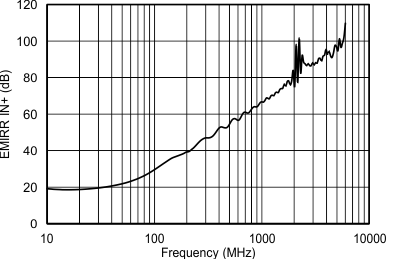
The robust design of the TLVx313-Q1 devices provides ease-of-use to the circuit designer: unity-gain stability with capacitive loads of up to 100 pF, integrated RFI/EMI rejection filter, no phase reversal in overdrive conditions, and high electrostatic discharge (ESD) protection (4-kV HBM).
The devices are optimized for operation at voltages as low as 1.8 V (±0.9 V) and up to 5.5 V (±2.75 V), and are specified over the extended temperature range of –40°C to +125°C.
The single-channel TLV313-Q1 device is available in an SC70-5 package.The dual-channel TLV2313-Q1 device is offered in SOIC-8 (D) and VSSOP-8 (DGK) packages.
Device Information(1)
| PART NUMBER | PACKAGE | BODY SIZE (NOM) |
|---|---|---|
| TLV313-Q1 | SC70 (5) | 2.00 mm × 1.25 mm |
| TLV2313-Q1 | SOIC (8) | 4.90 mm × 3.91 mm |
| VSSOP (8) | 3.00 mm × 3.00 mm |
- For all available packages, see the orderable addendum at the end of the data sheet.
EMIRR IN+ vs Frequency
