SBOS884A October 2017 – December 2018 TLV2313-Q1 , TLV313-Q1
PRODUCTION DATA.
- 1 Features
- 2 Applications
- 3 Description
- 4 Revision History
- 5 Device Comparison Table
- 6 Pin Configuration and Functions
-
7 Specifications
- 7.1 Absolute Maximum Ratings
- 7.2 ESD Ratings
- 7.3 Recommended Operating Conditions
- 7.4 Thermal Information: TLV313-Q1
- 7.5 Thermal Information: TLV2313-Q1
- 7.6 Electrical Characteristics: 5.5 V
- 7.7 Electrical Characteristics: 1.8 V
- 7.8 Typical Characteristics: Table of Graphs
- 7.9 Typical Characteristics
- 8 Detailed Description
- 9 Application and Implementation
- 10Power Supply Recommendations
- 11Layout
- 12Device and Documentation Support
- 13Mechanical, Packaging, and Orderable Information
Package Options
Mechanical Data (Package|Pins)
Thermal pad, mechanical data (Package|Pins)
Orderable Information
9.2 Typical Application
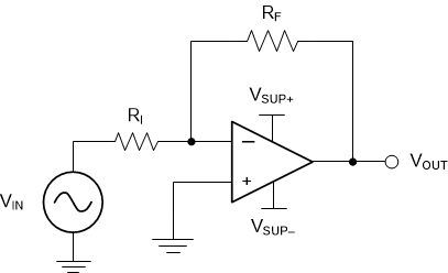
A typical application for an operational amplifier is an inverting amplifier, as shown in Figure 21. An inverting amplifier takes a positive voltage on the input and outputs a signal inverted to the input, making a negative voltage of the same magnitude. In the same manner, the amplifier also makes negative input voltages positive on the output. In addition, amplification may be added by selecting the input resistor (RI) and the feedback resistor (RF.)
 Figure 21. Application Schematic