SBOS837A November   2016  – January 2019 TLV2314-Q1 , TLV314-Q1 , TLV4314-Q1

PRODUCTION DATA.  

  1. Features
  2. Applications
  3. Description
    1.     Device Images
      1.      EMIRR vs Frequency
  4. Revision History
  5. Pin Configuration and Functions
    1.     Pin Functions: TLV314-Q1
    2.     Pin Functions: TLV2314-Q1
    3.     Pin Functions: TLV4314-Q1
  6. Specifications
    1. 6.1 Absolute Maximum Ratings
    2. 6.2 ESD Ratings
    3. 6.3 Recommended Operating Conditions
    4. 6.4 Thermal Information: TLV314-Q1
    5. 6.5 Thermal Information: TLV2314-Q1
    6. 6.6 Thermal Information: TLV4314-Q1
    7. 6.7 Electrical Characteristics
    8. 6.8 Typical Characteristics
    9. 6.9 Typical Characteristics
  7. Detailed Description
    1. 7.1 Overview
    2. 7.2 Functional Block Diagram
    3. 7.3 Feature Description
      1. 7.3.1 Operating Voltage
      2. 7.3.2 Rail-to-Rail Input
      3. 7.3.3 Rail-to-Rail Output
      4. 7.3.4 Common-Mode Rejection Ratio (CMRR)
      5. 7.3.5 Capacitive Load and Stability
      6. 7.3.6 EMI Susceptibility and Input Filtering
    4. 7.4 Device Functional Modes
  8. Application and Implementation
    1. 8.1 Application Information
    2. 8.2 Typical Application
      1. 8.2.1 Design Requirements
      2. 8.2.2 Detailed Design Procedure
      3. 8.2.3 Application Curve
    3. 8.3 System Examples
  9. Power Supply Recommendations
    1. 9.1 Input and ESD Protection
  10. 10Layout
    1. 10.1 Layout Guidelines
    2. 10.2 Layout Example
  11. 11Device and Documentation Support
    1. 11.1 Device Support
      1. 11.1.1 Development Support
    2. 11.2 Documentation Support
      1. 11.2.1 Related Documentation
    3. 11.3 Related Links
    4. 11.4 Community Resources
    5. 11.5 Trademarks
    6. 11.6 Electrostatic Discharge Caution
    7. 11.7 Glossary
  12. 12Mechanical, Packaging, and Orderable Information

Package Options

Mechanical Data (Package|Pins)
Thermal pad, mechanical data (Package|Pins)
Orderable Information

Typical Characteristics

at TA = 25°C, RL = 10 kΩ connected to VS / 2, VCM = VS / 2, and VOUT = VS / 2 (unless otherwise noted)
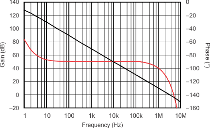
TLV314-Q1 TLV2314-Q1 TLV4314-Q1 tc_open_loop_gain_phase_fqcy_sbos754.gif
RL = 10 kΩ and 10 pF, VS = ±2.5 V
Figure 1. Open-Loop Gain and Phase vs Frequency
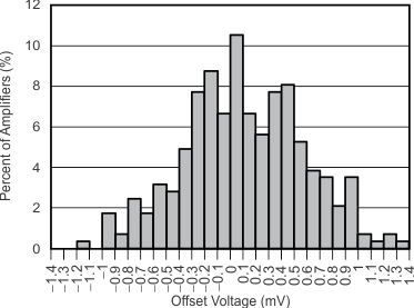
TLV314-Q1 TLV2314-Q1 TLV4314-Q1 tc_histo_voffset_sbos754.gif
Figure 3. Offset Voltage Production Distribution
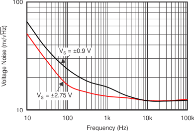
TLV314-Q1 TLV2314-Q1 TLV4314-Q1 tc_vin_spec_density_fqcy_bos563.gif
Figure 5. Input Voltage Noise Spectral Density vs
Frequency
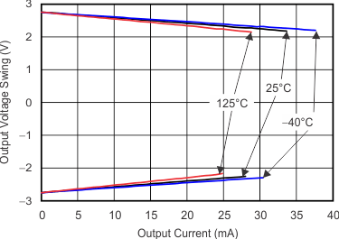
TLV314-Q1 TLV2314-Q1 TLV4314-Q1 tc_vout_swing_iout_sbos754.gif
VS = ±2.75 V
Figure 7. Output Voltage Swing vs Output Current
(Overtemperature)
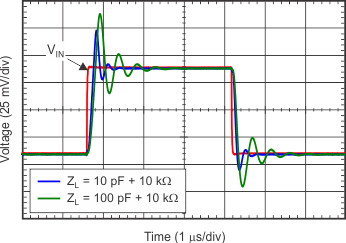
TLV314-Q1 TLV2314-Q1 TLV4314-Q1 tc_sm_sig_step_09V_sbos754.gif
VS = ±0.9 V Gain = 1 V/V RF = 10 kΩ
Figure 9. Small-Signal Pulse Response (Noninverting)
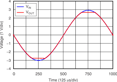
TLV314-Q1 TLV2314-Q1 TLV4314-Q1 tc_anti_phase_reversal_bos563.gif
Figure 11. No Phase Reversal
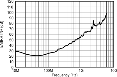
TLV314-Q1 TLV2314-Q1 TLV4314-Q1 tc_emirr_2314_sbos754.gif
PRF = –10 dBm VS = ±2.5 V VCM = 0 V
Figure 13. Electromagnetic Interference Rejection Ratio
Referred to Noninverting Input (EMIRR IN+) vs Frequency
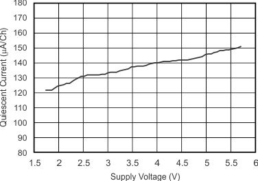
TLV314-Q1 TLV2314-Q1 TLV4314-Q1 tc_iq_vsupply_sbos754.gif
Figure 2. Quiescent Current vs Supply
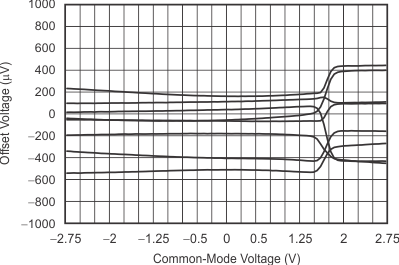
TLV314-Q1 TLV2314-Q1 TLV4314-Q1 tc_vos_vcm_sbos754.gif
Typical units, VS = ±2.75 V
Figure 4. Offset Voltage vs Common-Mode Voltage
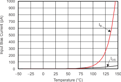
TLV314-Q1 TLV2314-Q1 TLV4314-Q1 tc_input_bias_temp_sbos754.gif
Figure 6. Input Bias and Offset Current vs Temperature
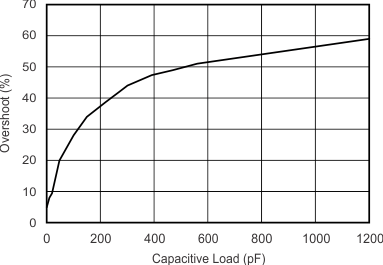
TLV314-Q1 TLV2314-Q1 TLV4314-Q1 tc_sm_sig_ovrsht_cap_load_sbos754.gif
VS = ±2.75 V Gain = 1 V/V RL = 10 kΩ
Figure 8. Small-Signal Overshoot vs Load Capacitance
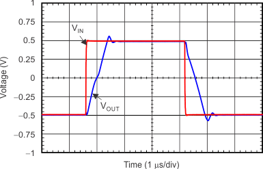
TLV314-Q1 TLV2314-Q1 TLV4314-Q1 tc_lg_sig_step_09V_sbos754.gif
VS = ±0.9 V Gain = 1 V/V RL = 10 kΩ
Figure 10. Large-Signal Pulse Response (Noninverting)
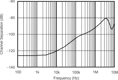
TLV314-Q1 TLV2314-Q1 TLV4314-Q1 tc_chan_separat_fqcy_sbos754.gif
VS = ±2.75 V
Figure 12. Channel Separation vs Frequency (TLV2314)