SLVSJH6B July   2025  – December 2025 TLV3214-Q1

PRODMIX  

  1.   1
  2. Features
  3. Applications
  4. Description
  5. Pin Configuration and Functions
    1. 4.1 Pin Configuration: TLV3211-Q1, TLV3221-Q1
    2. 4.2 Pin Configurations: TLV3212-Q1, TLV3222-Q1
    3. 4.3 Pin Configurations: TLV3214-Q1
  6. Specifications
    1. 5.1 Absolute Maximum Ratings
    2. 5.2 ESD Ratings
    3. 5.3 Recommended Operating Conditions
    4. 5.4 Thermal Information - Single
    5. 5.5 Thermal Information - Dual
    6. 5.6 Thermal Information - Quad
    7. 5.7 Electrical Characteristics
    8. 5.8 Switching Characteristics
    9. 5.9 Typical Characteristics
  7. Detailed Description
    1. 6.1 Overview
    2. 6.2 Functional Block Diagrams
    3. 6.3 Feature Description
    4. 6.4 Device Functional Modes
      1. 6.4.1 Inputs
        1. 6.4.1.1 Unused Inputs
      2. 6.4.2 Internal Hysteresis
      3. 6.4.3 Outputs
        1. 6.4.3.1 Push-Pull Output
        2. 6.4.3.2 Open Drain Output
      4. 6.4.4 ESD Protection
      5. 6.4.5 Power-On Reset (POR)
  8. Application and Implementation
    1. 7.1 Application Information
      1. 7.1.1 Basic Comparator Definitions
        1. 7.1.1.1 Operation
        2. 7.1.1.2 Propagation Delay
        3. 7.1.1.3 Overdrive Voltage
      2. 7.1.2 External Hysteresis
        1. 7.1.2.1 Inverting Comparator With Hysteresis
        2. 7.1.2.2 Non-Inverting Comparator With Hysteresis
    2. 7.2 Typical Applications
      1. 7.2.1 Low-Side Current Sensing
        1. 7.2.1.1 Design Requirements
        2. 7.2.1.2 Detailed Design Procedure
    3. 7.3 Power Supply Recommendations
    4. 7.4 Layout
      1. 7.4.1 Layout Guidelines
      2. 7.4.2 Layout Example
  9. Device and Documentation Support
    1. 8.1 Documentation Support
      1. 8.1.1 Related Documentation
    2. 8.2 Receiving Notification of Documentation Updates
    3. 8.3 Support Resources
    4. 8.4 Trademarks
    5. 8.5 Electrostatic Discharge Caution
    6. 8.6 Glossary
  10. Revision History
  11. 10Mechanical, Packaging, and Orderable Information

Package Options

Mechanical Data (Package|Pins)
Thermal pad, mechanical data (Package|Pins)
Orderable Information

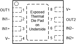
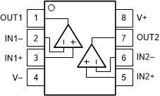
Pin Configurations: TLV3212-Q1, TLV3222-Q1

TLV3211-Q1 TLV3212-Q1 TLV3214-Q1 TLV3221-Q1 TLV3222-Q1 D, DGK Packages8-Pin SOIC,
                            VSSOPTop
                            ViewD, DGK Packages
8-Pin SOIC, VSSOP
Top View
TLV3211-Q1 TLV3212-Q1 TLV3214-Q1 TLV3221-Q1 TLV3222-Q1 DSG Package8-Pad WSON With Exposed Thermal
                            PadTop
                            View
NOTE: Connect exposed thermal pad directly to V- pin.
DSG Package
8-Pad WSON With Exposed Thermal Pad
Top View
Table 4-2 Pin Functions: TLV3212-Q1, TLV3222-Q1
PIN TYPE(1) DESCRIPTION
NAME NO.
OUT1 1 O Output pin of the comparator 1
IN1– 2 I Inverting input pin of comparator 1
IN1+ 3 I Noninverting input pin of comparator 1
V- 4 Negative supply voltage
IN2+ 5 I Noninverting input pin of comparator 2
IN2– 6 I Inverting input pin of comparator 2
OUT2 7 O Output pin of the comparator 2
V+ 8 Positive supply voltage
Thermal Pad Connect directly to V- pin
I = input, O = output