SNOSDL8B November 2024 – November 2025 TLV3511-Q1 , TLV3512-Q1
PRODMIX
- 1
- 1 Features
- 2 Applications
- 3 Description
- 4 Pin Configuration and Functions
- 5 Specifications
- 6 Detailed Description
- 7 Application and Implementation
- 8 Device and Documentation Support
- 9 Revision History
- 10Mechanical, Packaging, and Orderable Information
Package Options
Mechanical Data (Package|Pins)
- DGK|8
Thermal pad, mechanical data (Package|Pins)
Orderable Information
3 Description
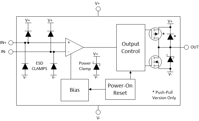
The TLV351x-Q1 is a family of 5V single and dual channel comparators with push-pull outputs. The family has an excellent speed-to-power combination with a propagation delay of 6ns and a full supply voltage range of 2.7V to 5.5V with a quiescent supply current of only 1mA per channel.
All devices include a Power-On Reset (POR) feature. This makes sure the output is in a known state (output LOW) until the minimum supply voltage has been reached before the output responds to the inputs, thus preventing false outputs during system power-up and power-down.Likewise, the TLV351x-Q1 are conveniently available in standard leaded and leadless packages with features such as rail-to-rail inputs, low offset voltage, and large output drive current. These features along with fast response time make the comparators well-suited for current sensing, zero-cross detection, and a variety of other applications where precision and speed is critical.
All devices operate across the expanded temperature range of –40°C to 125°C.
| PART NUMBER | PACKAGE(1) | PACKAGE SIZE(2) |
|---|---|---|
| TLV3511-Q1 | DCK (SC-70, 5) | 2mm × 2.1mm |
| DBV (SOT-23, 5) | 2.9mm × 2.8mm | |
| DRL (SOT, 5) (Preview) | 1.6mm × 1.6mm | |
| TLV3512-Q1 | DGK (VSSOP, 8) | 3.00mm × 4.9mm |
| DSG (WSON, 8) (Preview) | 2.00mm × 2.00mm |
 Block Diagram
 Low-Side Current Sensing