SBVS401B June   2020  – August 2025 TLV740P

PRODUCTION DATA  

  1.   1
  2. Features
  3. Applications
  4. Description
  5. Pin Configuration and Functions
  6. Specifications
    1. 5.1 Absolute Maximum Ratings
    2. 5.2 ESD Ratings
    3. 5.3 Recommended Operating Conditions
    4. 5.4 Thermal Information
    5. 5.5 Electrical Characteristics
    6. 5.6 Typical Characteristics
  7. Detailed Description
    1. 6.1 Overview
    2. 6.2 Functional Block Diagram
    3. 6.3 Feature Description
      1. 6.3.1 Foldback Current Limit
      2. 6.3.2 Output Enable
      3. 6.3.3 Active Discharge
      4. 6.3.4 Undervoltage Lockout (UVLO) Operation
      5. 6.3.5 Dropout Voltage
      6. 6.3.6 Thermal Shutdown
    4. 6.4 Device Functional Modes
      1. 6.4.1 Device Functional Mode Comparison
      2. 6.4.2 Normal Operation
      3. 6.4.3 Dropout Operation
      4. 6.4.4 Disabled
  8. Application and Implementation
    1. 7.1 Application Information
      1. 7.1.1 Recommended Capacitor Types
      2. 7.1.2 Input and Output Capacitor Requirements
      3. 7.1.3 Dropout Voltage
      4. 7.1.4 Exiting Dropout
      5. 7.1.5 Transient Response
      6. 7.1.6 Reverse Current
      7. 7.1.7 Power Dissipation (PD)
        1. 7.1.7.1 Estimating Junction Temperature
        2. 7.1.7.2 Recommended Area for Continuous Operation
    2. 7.2 Typical Application
      1. 7.2.1 Design Requirements
      2. 7.2.2 Detailed Design Procedure
      3. 7.2.3 Application Curves
    3. 7.3 Best Design Practices
    4. 7.4 Power Supply Recommendations
    5. 7.5 Layout
      1. 7.5.1 Layout Guidelines
      2. 7.5.2 Layout Examples
  9. Device and Documentation Support
    1. 8.1 Device Support
      1. 8.1.1 Development Support
        1. 8.1.1.1 Device Nomenclature
    2. 8.2 Documentation Support
      1. 8.2.1 Related Documentation
    3. 8.3 Receiving Notification of Documentation Updates
    4. 8.4 Support Resources
    5. 8.5 Trademarks
    6. 8.6 Electrostatic Discharge Caution
    7. 8.7 Glossary
  10. Revision History
  11. 10Mechanical, Packaging, and Orderable Information

Package Options

Mechanical Data (Package|Pins)
Thermal pad, mechanical data (Package|Pins)
Orderable Information

Typical Characteristics

over operating temperature range (TJ = –40°C to 85°C), VIN = VOUT(nom) + 2.1 V, IOUT = 1 mA, VEN = VIN, and CIN = COUT = 1 µF (unless otherwise noted); typical values are at TJ = 25°C

TLV740 TLV740P Line Regulation vs VIN
Figure 5-1 Line Regulation vs VIN
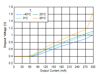
TLV740 TLV740P Dropout Voltage vs IOUT
VOUT = 1.0 V
Figure 5-3 Dropout Voltage vs IOUT
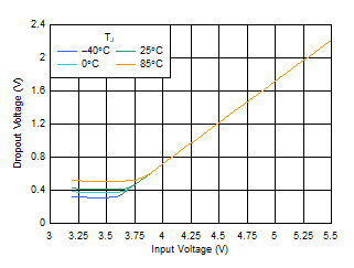
TLV740 TLV740P Dropout Voltage vs VIN
VOUT = 1.0 V
Figure 5-5 Dropout Voltage vs VIN
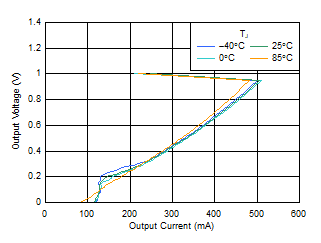
TLV740 TLV740P Foldback Current Limit vs IOUT
VOUT = 1.0 V
Figure 5-7 Foldback Current Limit vs IOUT
TLV740 TLV740P Foldback Current Limit vs IOUT
VOUT = 3.3 V
Figure 5-9 Foldback Current Limit vs IOUT
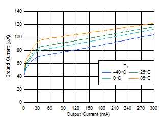
TLV740 TLV740P IGND vs IOUT
VOUT = 3.3 V
Figure 5-11 IGND vs IOUT
TLV740 TLV740P UVLO Rising and Falling Threshold vs Temperature
 
Figure 5-13 UVLO Rising and Falling Threshold vs Temperature
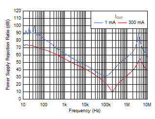
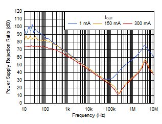
TLV740 TLV740P PSRR vs Frequency and IOUT
CIN = open, VOUT = 1.8 V
Figure 5-15 PSRR vs Frequency and IOUT
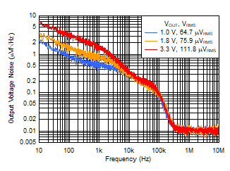
TLV740 TLV740P Output Noise vs Frequency and VOUT
 
Figure 5-17 Output Noise vs Frequency and VOUT
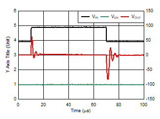
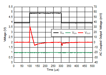
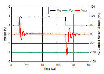
TLV740 TLV740P Line
                        Transient
VIN = 3.9 V to 4.9 V, slew rate = 1 V/µs, VEN = 1 V,
IOUT = 150 mA
Figure 5-19 Line Transient
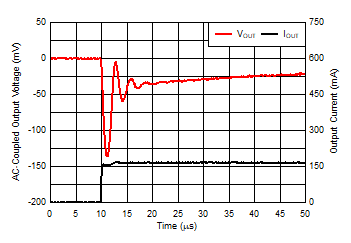
TLV740 TLV740P Load
                        Transient
VIN = 3.9 V, VEN = 1 V, IOUT = 1 mA to 150 mA,
slew rate = 1 A/µs
Figure 5-21 Load Transient
TLV740 TLV740P Load
                        Transient
VIN = 3.9 V, VEN = 1 V, IOUT = 1 mA to 300 mA,
slew rate = 1 A/µs
Figure 5-23 Load Transient
TLV740 TLV740P Start-Up With EN, Inrush Current
VIN = 5.5 V, CIN = open, IOUT = open
Figure 5-25 Start-Up With EN, Inrush Current
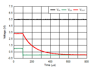
TLV740 TLV740P Shutdown Response With Enable
VIN = 5.5 V, VEN = 1 V to 0 V, IOUT = open
Figure 5-27 Shutdown Response With Enable
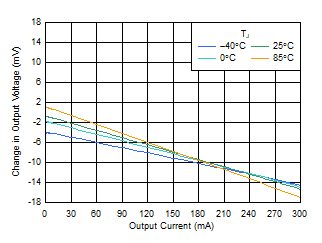
TLV740 TLV740P Load
                        Regulation vs IOUT
Figure 5-2 Load Regulation vs IOUT
TLV740 TLV740P Dropout Voltage vs IOUT
VOUT = 3.3 V
Figure 5-4 Dropout Voltage vs IOUT
TLV740 TLV740P Dropout Voltage vs VIN
VOUT = 3.3 V
Figure 5-6 Dropout Voltage vs VIN
TLV740 TLV740P Foldback Current Limit vs IOUT
VOUT = 1.8 V
Figure 5-8 Foldback Current Limit vs IOUT
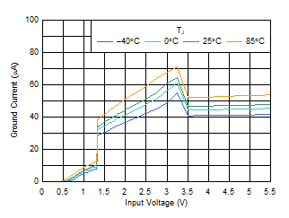
TLV740 TLV740P IGND vs VIN
VOUT = 3.3 V, IOUT = 0 mA
Figure 5-10 IGND vs VIN
TLV740 TLV740P EN High and Low Threshold vs Temperature
VIN = 5.5 V
Figure 5-12 EN High and Low Threshold vs Temperature
TLV740 TLV740P PSRR vs Frequency and IOUT
CIN = open, VOUT = 1.0 V
Figure 5-14 PSRR vs Frequency and IOUT
TLV740 TLV740P PSRR vs Frequency and IOUT
CIN = open, VOUT = 3.3 V
Figure 5-16 PSRR vs Frequency and IOUT
TLV740 TLV740P Line Transient
VIN = 3.9 V to 4.9 V, slew rate = 1 V/µs, VEN = 1 V, IOUT = 1 mA
Figure 5-18 Line Transient
TLV740 TLV740P Line
                        Transient
VIN = 3.9 V to 4.9 V, slew rate = 1 V/µs, VEN = 1 V,
IOUT = 300 mA
Figure 5-20 Line Transient
TLV740 TLV740P Load
                        Transient
VIN = 3.9 V, VEN = 1 V, IOUT = 1 mA to 150 mA,
slew rate = 1 A/µs, rising edge
Figure 5-22 Load Transient
TLV740 TLV740P Load
                        Transient
VIN = 3.9 V, VEN = 1 V, IOUT = 1 mA to 300 mA,
slew rate = 1 A/µs, rising edge
Figure 5-24 Load Transient
TLV740 TLV740P Start-Up and Shutdown
VIN = 0 V to 5.5 V to 0 V, IOUT = 150 mA
Figure 5-26 Start-Up and Shutdown