SBVS401B June   2020  – August 2025 TLV740P

PRODUCTION DATA  

  1.   1
  2. Features
  3. Applications
  4. Description
  5. Pin Configuration and Functions
  6. Specifications
    1. 5.1 Absolute Maximum Ratings
    2. 5.2 ESD Ratings
    3. 5.3 Recommended Operating Conditions
    4. 5.4 Thermal Information
    5. 5.5 Electrical Characteristics
    6. 5.6 Typical Characteristics
  7. Detailed Description
    1. 6.1 Overview
    2. 6.2 Functional Block Diagram
    3. 6.3 Feature Description
      1. 6.3.1 Foldback Current Limit
      2. 6.3.2 Output Enable
      3. 6.3.3 Active Discharge
      4. 6.3.4 Undervoltage Lockout (UVLO) Operation
      5. 6.3.5 Dropout Voltage
      6. 6.3.6 Thermal Shutdown
    4. 6.4 Device Functional Modes
      1. 6.4.1 Device Functional Mode Comparison
      2. 6.4.2 Normal Operation
      3. 6.4.3 Dropout Operation
      4. 6.4.4 Disabled
  8. Application and Implementation
    1. 7.1 Application Information
      1. 7.1.1 Recommended Capacitor Types
      2. 7.1.2 Input and Output Capacitor Requirements
      3. 7.1.3 Dropout Voltage
      4. 7.1.4 Exiting Dropout
      5. 7.1.5 Transient Response
      6. 7.1.6 Reverse Current
      7. 7.1.7 Power Dissipation (PD)
        1. 7.1.7.1 Estimating Junction Temperature
        2. 7.1.7.2 Recommended Area for Continuous Operation
    2. 7.2 Typical Application
      1. 7.2.1 Design Requirements
      2. 7.2.2 Detailed Design Procedure
      3. 7.2.3 Application Curves
    3. 7.3 Best Design Practices
    4. 7.4 Power Supply Recommendations
    5. 7.5 Layout
      1. 7.5.1 Layout Guidelines
      2. 7.5.2 Layout Examples
  9. Device and Documentation Support
    1. 8.1 Device Support
      1. 8.1.1 Development Support
        1. 8.1.1.1 Device Nomenclature
    2. 8.2 Documentation Support
      1. 8.2.1 Related Documentation
    3. 8.3 Receiving Notification of Documentation Updates
    4. 8.4 Support Resources
    5. 8.5 Trademarks
    6. 8.6 Electrostatic Discharge Caution
    7. 8.7 Glossary
  10. Revision History
  11. 10Mechanical, Packaging, and Orderable Information

Package Options

Mechanical Data (Package|Pins)
Thermal pad, mechanical data (Package|Pins)
Orderable Information

Description

The TLV740P low-dropout (LDO) linear regulator is a low quiescent current LDO with excellent line and load transient performance designed for power-sensitive applications. This device provides a typical accuracy of 1%.

The TLV740P also provides inrush current control during device power up and enabling. The TLV740P limits the input current to the defined current limit to avoid large currents from flowing from the input power source. This functionality is especially important in battery-operated devices.

The TLV740P is available in standard DQN and DBV packages. The TLV740P also provides an active pulldown circuit to quickly discharge output loads.

Package Information
PART NUMBER PACKAGE(1) PACKAGE SIZE(2)
TLV740, TLV740P DBV (SOT-23, 5) 2.9mm × 2.8mm
DQN (X2SON, 4) 1mm × 1mm
For more information, see the Mechanical, Packaging, and Orderable Information.
The package size (length × width) is a nominal value and includes pins, where applicable.
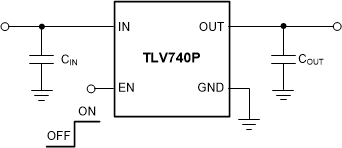
TLV740 TLV740P Typical Application
                        CircuitTypical Application Circuit
TLV740 TLV740P Dropout Voltage vs Output Current
                            (3.3VOUT)Dropout Voltage vs Output Current (3.3VOUT)