SBOS836G March 2020 – March 2022 TLV9041 , TLV9042 , TLV9044
PRODUCTION DATA
- 1 Features
- 2 Applications
- 3 Description
- 4 Revision History
- 5 Device Comparison Table
- 6 Pin Configuration and Functions
- 7 Specifications
-
8 Detailed Description
- 8.1 Overview
- 8.2 Functional Block Diagram
- 8.3
Feature Description
- 8.3.1 Operating Voltage
- 8.3.2 Rail-to-Rail Input
- 8.3.3 Rail-to-Rail Output
- 8.3.4 Common-Mode Rejection Ratio (CMRR)
- 8.3.5 Capacitive Load and Stability
- 8.3.6 Overload Recovery
- 8.3.7 EMI Rejection
- 8.3.8 Electrical Overstress
- 8.3.9 Input and ESD Protection
- 8.3.10 Shutdown Function
- 8.3.11 Packages With an Exposed Thermal Pad
- 8.4 Device Functional Modes
- 9 Application and Implementation
- 10Power Supply Recommendations
- 11Layout
- 12Device and Documentation Support
- 13Mechanical, Packaging, and Orderable Information
Package Options
Mechanical Data (Package|Pins)
Thermal pad, mechanical data (Package|Pins)
- DPW|5
Orderable Information
8.3.5 Capacitive Load and Stability
The TLV904x is designed to be used in applications where driving a capacitive load is required. As with all operational amplifiers, there may be specific instances where the TLV904x can become unstable. The particular operational amplifier circuit configuration, layout, gain, and output loading are some of the factors to consider when establishing whether or not an amplifier is stable in operation. An operational amplifier in the unity-gain (1 V/V) buffer configuration that drives a capacitive load exhibits a greater tendency to be unstable than an amplifier operated at a higher noise gain. The capacitive load, in conjunction with the operational amplifier output resistance, creates a pole within the feedback loop that degrades the phase margin. The degradation of the phase margin increases when capacitive loading increases. When operating in the unity-gain configuration, the TLV904x remains stable with a pure capacitive load up to approximately 100 pF with a good phase margin of 45° typical. The equivalent series resistance (ESR) of some very large capacitors (CL greater than 1 μF) is sufficient to alter the phase characteristics in the feedback loop such that the amplifier remains stable. Increasing the amplifier closed-loop gain allows the amplifier to drive increasingly larger capacitance. This increased capability is evident when measuring the overshoot response of the amplifier at higher voltage gains.
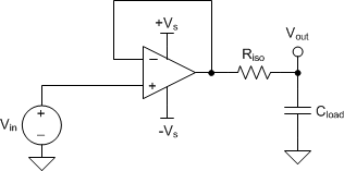
One technique for increasing the capacitive load drive capability of the amplifier operating in a unity-gain configuration is to insert a small resistor (typically 10 Ω to 20 Ω) in series with the output, as shown in Figure 8-3. This resistor significantly reduces the overshoot and ringing associated with large capacitive loads. One possible problem with this technique, however, is that a voltage divider is created with the added series resistor and any resistor connected in parallel with the capacitive load. The voltage divider introduces a gain error at the output that reduces the output swing.
 Figure 8-3 Improving
Capacitive Load Drive