SNVSCI2B February 2023 – February 2024 TLVM23615 , TLVM23625
PRODUCTION DATA
- 1
- 1 Features
- 2 Applications
- 3 Description
- 4 Device Comparison Table
- 5 Pin Configuration and Functions
- 6 Specifications
-
7 Detailed Description
- 7.1 Overview
- 7.2 Functional Block Diagram
- 7.3
Feature Description
- 7.3.1 Input Voltage Range
- 7.3.2 Output Voltage Selection
- 7.3.3 Input Capacitors
- 7.3.4 Output Capacitors
- 7.3.5 Enable, Start-Up, and Shutdown
- 7.3.6 Switching Frequency (RT)
- 7.3.7 Power-Good Output Operation
- 7.3.8 Internal LDO, VCC and VOUT/FB Input
- 7.3.9 Bootstrap Voltage and VBOOT-UVLO (BOOT Terminal)
- 7.3.10 Soft Start and Recovery from Dropout
- 7.3.11 Overcurrent Protection (Hiccup Mode)
- 7.3.12 Thermal Shutdown
- 7.4 Device Functional Modes
-
8 Application and Implementation
- 8.1 Application Information
- 8.2
Typical Application
- 8.2.1 Design Requirements
- 8.2.2
Detailed Design Procedure
- 8.2.2.1 Custom Design With WEBENCH® Tools
- 8.2.2.2 Choosing the Switching Frequency
- 8.2.2.3 Setting the Output Voltage
- 8.2.2.4 Input Capacitor Selection
- 8.2.2.5 Output Capacitor Selection
- 8.2.2.6 VCC
- 8.2.2.7 CFF Selection
- 8.2.2.8 Power-Good Signal
- 8.2.2.9 Maximum Ambient Temperature
- 8.2.2.10 Other Connections
- 8.2.3 Application Curves
- 8.3 Best Design Practices
- 8.4 Power Supply Recommendations
- 8.5 Layout
- 9 Device and Documentation Support
- 10Revision History
- 11Mechanical, Packaging, and Orderable Information
Package Options
Mechanical Data (Package|Pins)
- RDN|11
Thermal pad, mechanical data (Package|Pins)
- RDN|11
Orderable Information
7.3.5 Enable, Start-Up, and Shutdown
Voltage at the EN pin controls the start-up or remote shutdown of the TLVM236x5. The part stays shut down as long as the EN pin voltage is less than VEN-WAKE.With the voltage at the EN pin greater than VEN-WAKE, the device enters device standby mode and the internal LDO powers up to generate VCC. As the EN voltage increases further, approaching VEN-RISE, the device finally starts to switch, entering start-up mode with a soft start. During the device shutdown process, when the EN input voltage measures less than (VEN-RISE–VEN-HYST), the regulator stops switching and re-enters device standby mode. Any further decrease in the EN pin voltage, below VEN-WAKE, and the device is then firmly shut down. The high-voltage compliant EN input pin can be connected directly to the VIN input pin if remote precision control is not needed. The EN input pin must not be allowed to float.
The various EN threshold parameters and their values are listed in the Electrical Characteristics. Figure 7-3 shows the precision enable behavior and Figure 7-4 shows a typical remote EN start-up waveform in an application. After EN goes high, after a delay of about 1 ms, the output voltage begins to rise with a soft start and reaches close to the final value in about 3.5 ms (tss). After a delay of about 2.5 ms (tPG_FLT_RISE), the PGOOD flag goes high. During start-up, the device is not allowed to enter FPWM mode until the soft-start time has elapsed. This time is measured from the rising edge of EN.
 Figure 7-3 Precision Enable
Behavior
 Figure 7-4 Enable Start-Up VIN
= 24 V, VOUT = 3.3 V, IOUT = 2.5 A
Figure 7-4 Enable Start-Up VIN
= 24 V, VOUT = 3.3 V, IOUT = 2.5 AExternal UVLO through EN Pin
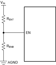
In some cases, an input UVLO level different than that provided internal to the device is needed. This can be accomplished by using the circuit shown in Figure 7-5. The input voltage at which the device turns on is designated as VON while the turn-off voltage is VOFF. First, a value for RENB is chosen in the range of 10 kΩ to 100 kΩ, then Equation 7and Equation 8 are used to calculate RENT and VOFF, respectively.
 Figure 7-5 Setup for
External UVLO Application
Figure 7-5 Setup for
External UVLO Applicationwhere
- VON is the VIN turn-on voltage.
- VOFF is the VIN turn-off voltage.
- Refer to electrical characteristics table for other terms.