SLASE75D August 2015 – September 2017 TMDS181
PRODUCTION DATA.
- 1 Features
- 2 Applications
- 3 Description
- 4 Revision History
- 5 Pin Configuration and Functions
-
6 Specifications
- 6.1 Absolute Maximum Ratings
- 6.2 ESD Ratings
- 6.3 Recommended Operating Conditions
- 6.4 Thermal Information
- 6.5 Power Supply Electrical Characteristics
- 6.6 TMDS Differential Input Electrical Characteristics
- 6.7 TMDS Differential Output Electrical Characteristics
- 6.8 DDC, I2C, HPD, and ARC Electrical Characteristics
- 6.9 Power-Up and Operation Timing Requirements
- 6.10 TMDS Switching Characteristics
- 6.11 HPD Switching Characteristics
- 6.12 DDC and I2C Switching Characteristics
- 6.13 Typical Characteristics
- 7 Parameter Measurement Information
-
8 Detailed Description
- 8.1 Overview
- 8.2 Functional Block Diagram
- 8.3
Feature Description
- 8.3.1 Reset Implementation
- 8.3.2 Operation Timing
- 8.3.3 Swap and Polarity Working
- 8.3.4 TMDS Inputs
- 8.3.5 TMDS Inputs Debug Tools
- 8.3.6 Receiver Equalizer
- 8.3.7 Input Signal Detect Block
- 8.3.8 Audio Return Channel
- 8.3.9 Transmitter Impedance Control
- 8.3.10 TMDS Outputs
- 8.3.11 Pre-Emphasis/De-Emphasis
- 8.4 Device Functional Modes
- 8.5 Register Maps
- 9 Application and Implementation
- 10Power Supply Recommendations
- 11Layout
- 12Device and Documentation Support
- 13Mechanical, Packaging, and Orderable Information
Package Options
Mechanical Data (Package|Pins)
- RGZ|48
Thermal pad, mechanical data (Package|Pins)
- RGZ|48
Orderable Information
8 Detailed Description
8.1 Overview
The TMDS181 is a DVI or HDMI™ retimer. The TMDS181 supports four TMDS channels, audio return channel (SPDIF_IN/ARC_OUT), hot plug detect, and DDC interfaces. The TMDS181 supports signaling rates up to 6 Gbps in retimer mode to allow for the highest resolutions of 4k2k60p 24 bits per pixel and up to WUXGA 16-bit color depth or 1080p with higher refresh rates. In redriver mode it supports HDMI1.4b with data rates up to 3.4 Gbps. The TMDS181 can be configured to support the HDMI2.0a standard which includes higher data rate, lower clock swing, and clock frequency. The TMDS181 can automatically configure itself as a redriver at low data rate (<1.0 Gbps) or as a retimer above this data rate. For passing compliance and reducing system-level design issues, several features are included such as TMDS output amplitude adjust using an external resistor on the VSADJ pin and source termination selection control. Device operation and configuration can be programmed by pin strapping or I2C. Four TMDS181s can be used on one I2C bus when I2C_EN enable and device address set by A0/A1.
To reduce active power, the TMDS181 supports dual power supply rails of 1.2 V on VDD and 3.3 V on VCC. There are several methods of power management, such as going into power-down mode using three methods:
- HPD is low
- Writing a 1 to register 09h[3]
- De-asserting OE
De-asserting OE clears the I2C registers, thus once reasserted the device must be reprogrammed if I2C was used for device setup. Upon return to normal active operation from reasserted OE or reasserted HPD, the TMDS181 requires the source to write a 1 to the TMDS_CLOCK_RATIO_STATUS bit for the TMDS181 to resume 1/40th clock mode. The TMDS181 does not reset this bit based upon a DDC read transaction. The SIG_EN pin enables the signal detect circuit that provides an automatic power-management feature during normal operation. When no valid signal is present on the inputs, the device will enter standby mode. By disabling the detect circuit, the receiver block is always on. DDC bridge supports the HDMI2.0 SCDC communication, 100 Kbps data rate default and 400 kbps adjustable by software.
TMDS181 supports both fixed EQ gain control or adaptive equalization to compensate for different lengths of input cables or board traces. The EQ gain can be software adjusted by I2C control or selection between two fixed values or adaptive (Retimer Mode Only) equalization by pin strapping EQ_SEL pin. The customer can pull up or down TX_TERM_CTL through a 65 kΩ resistor to change the termination impedance for improved output performance when working in HDMI1.4b or leave it not connected. When not connected, the TMDS181 in conjunction with the rate detect automatically changes its output termination to meet HDMI1.4b or HDMI2.0a needs. For HDMI1.4b a transmitter termination of 150 Ω to 300 Ω is allowed for data rates above 2 Gbps to compensate for reflections. The automatic termination selection will configure the TMDS181 for this. It is important to note that there are times that this is not the best solution and no termination may be needed to pass compliance. For HDMI2.0a the 75 Ω to 150 Ω transmitter termination is required and the link will not work if this is not set.
The TMDS181 supports the audio return channel to support HDMI1.4b. To make implementation easier, the TMDS181 supports input pin swapping and input polarity swap. When swapping the input pins, IN_CLK and IN_D2 swap and IN_D1 and IN_D0 swap with each other. Swap works in both retimer and redriver mode. Polarity swap exchanges the N and P channel polarity in each input lane and is only available during retimer mode. Lane swap and polarity swap can be implemented at the same time in retimer mode.
Two temperature gradient versions of the device are available: extended commercial temperature range 0ºC to 85ºC (TMDS181) and industrial temperature range from –40ºC to 85ºC (TMDS181I).
8.2 Functional Block Diagram
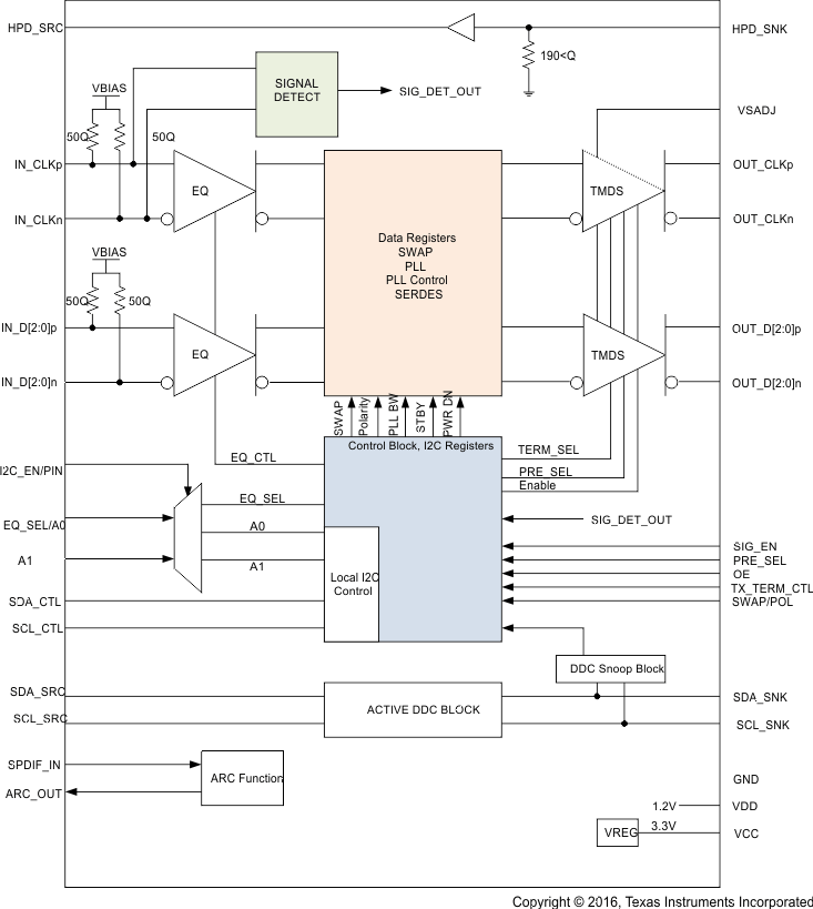
8.3 Feature Description
8.3.1 Reset Implementation
When OE is de-asserted, control signal inputs are ignored; the HDMI inputs and outputs are high impedance. It is critical to transition the OE from a low level to a high level after the VCC supply has reached the minimum recommended operating voltage. Achieve this transition by a control signal to the OE input, or by an external capacitor connected between OE and GND. To ensure the TMDS181 is properly reset, the OE pin must be de-asserted for at least 100 μs before being asserted. When OE is reasserted, the TMDS181 must be reprogrammed if it was programmed by I2C and not pin strapping. When implementing the external capacitor, the size of the external capacitor depends on the power up ramp of the VCC supply, where a slower ramp-up results in a larger-value external capacitor. Refer to the latest reference schematic for TMDS181; consider approximately 200 nF capacitor as a reasonable first estimate for the size of the external capacitor. Figure 24 and Figure 25 show both OE implementations.
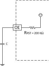 Figure 24. External Capacitor Controlled OE
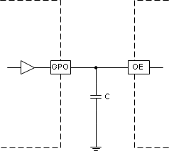 Figure 25. OE Input from Active Controller
8.3.2 Operation Timing
TMDS181 starts to operate after the OE signal is properly set after power-up timing completes. See Figure 1, Figure 2, and Power-Up and Operation Timing Requirements. If OE is held low until VDD and VCC become stable, there is no rail sequence requirement.
8.3.3 Swap and Polarity Working
TMDS181 incorporates swap function, which can set the input lanes in swap mode. The IN_D2 routes to the OUT_CLK position. The IN_D1 swaps with IN_D0. The swap function only changes the input pins. The EQ setup follows the new mapping (see Figure 26). This function can be used with the SWAP/POL pin 1 and control the register 0x09h bit 7 for SWAP enable. Lane swap function works in both redriver and retimer mode.
The TMDS181 can also swap the input polarity signals. When SWAP/POL is high the n and p pins on each lane will swap. Polarity swap only works when in retimer mode. Take care when this function is enabled and the device is in automatic crossover mode between redriver and retimer modes. When the data rate drops to the redriver level, the polarity swap is lost.
Table 2. SWAP Function(1)
| Normal Operation | SWAP = L or CSR 0x09h bit 7 is 1’b1 |
|---|---|
| IN_D2 → OUT_D2 | IN_D2 → OUT_CLK |
| IN_D1 → OUT_D1 | IN_D1 → OUT_D0 |
| IN_D0 → OUT_D0 | IN_D0 → OUT_D1 |
| IN_CLK → OUT_CLK | IN_CLK → OUT_D2 |
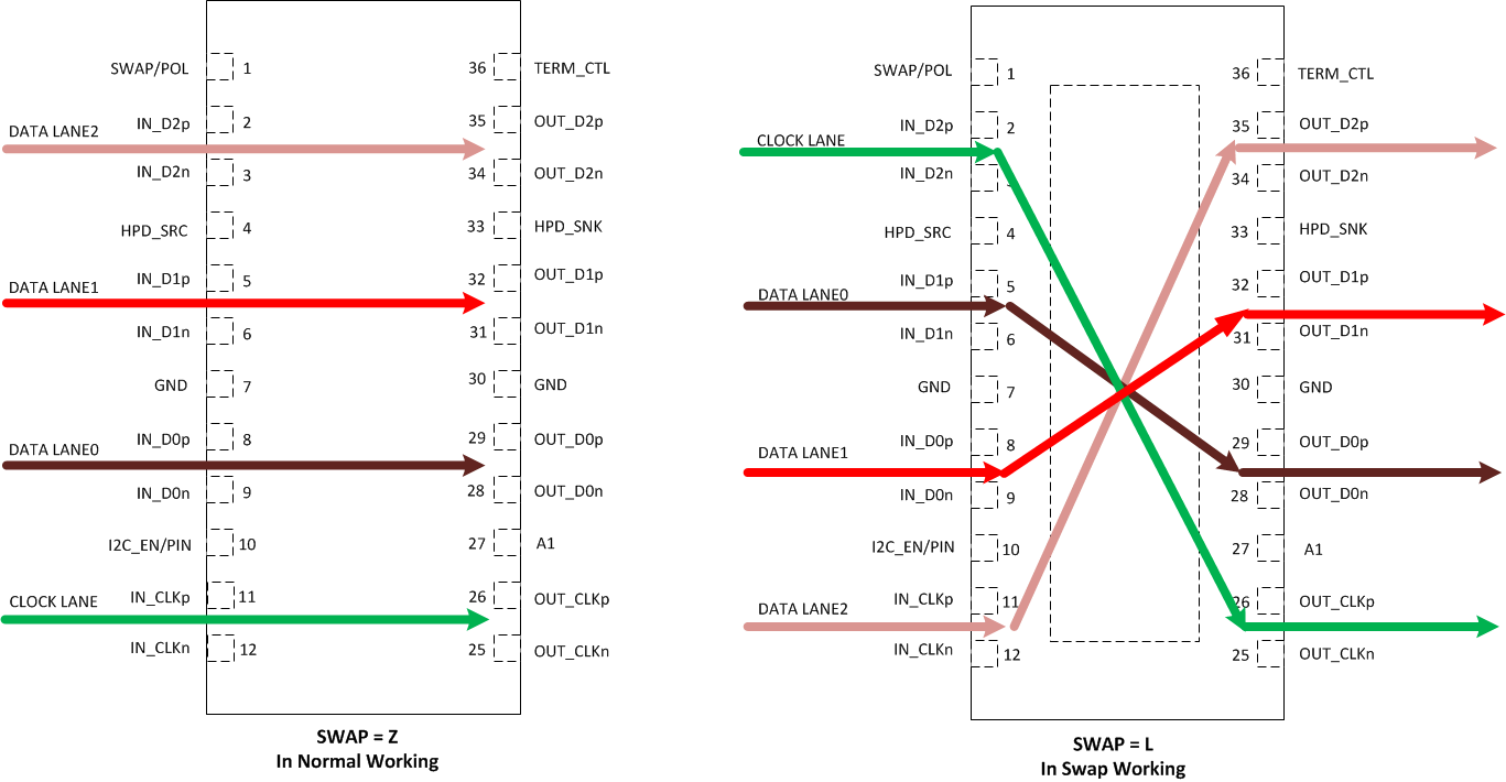 Figure 26. TMDS181 Swap Function
8.3.4 TMDS Inputs
Standard TMDS terminations are integrated on all TMDS inputs. External terminations are not required. Each input data channel contains an adaptive or fixed equalizer to compensate for cable or board losses. The voltage at the TMDS input pins must be limited below the absolute maximum ratings. An unused input should not be connected to ground because this would result in excessive current flow damaging the device. An unused input channel can be externally biased to prevent output oscillation. The complementary input pin is recommended to be grounded through a 1 kΩ resistor and the other pin left open. The input pins can be polarity changed through the local I2C register when in retimer mode.
8.3.5 TMDS Inputs Debug Tools
There are two methods for debugging a system to make sure the inputs to the TMDS181 are valid. A TMDS error checker is implemented to provide a rough bit error rate per data lane. This allows the system implementer to determine how the link between the source and TMDS181 is performing on all three data lanes. See RX PATTERN VERIFIER CONTROL/STATUS Register.
If a high error count is evident, the TMDS181 has a way to view the general eye quality. A tool is available that uses the I2C link to download the data that can be plotted for an eye diagram. This is available per data lane. This tool also provides a method to turn on an internal PRBS generator that will transmit a data signal on the data pins. A clock at the proper frequency is required on the IN_CLK pins to generate the expected output data rate.
8.3.6 Receiver Equalizer
Equalizers are used to clean up inter-symbol interference (ISI) jitter or loss from the bandwidth-limited board traces and cables. TMDS181 supports fixed receiver equalizer (Retimer and Redriver Mode) and adaptive receiver equalizer (Retimer Mode) by setting the EQ_SEL/A0 pin or through I2C reg0Ah[5]. When EQ_SEL/A0 is high, the EQ gain is fixed to 14 dB and when set low ,the EQ gain is set to 7.5 dB. TMDS181 operates in adaptive equalizer mode when the EQ_SEL/A0 pin is left floating. The EQ gain is automatically adjusted based on the data rate to compensate for trace or cable loss. Various fixed EQ values can be set through local I2C control, reg0Dh[5:1]. The fixed EQ value can be programmed for both the data and clock. Adaptive equalization is the default setting.
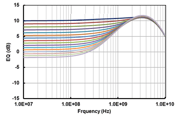 Figure 27. Adaptive EQ Gain Curve for >3.4 Gbps
8.3.7 Input Signal Detect Block
When SIG_EN is enabled, the TMDS looks for a valid TMDS clock signal input. The device is fully functional when a valid signal is detected. If no valid TMDS clock signal is detected, the device enters standby mode waiting for a valid signal at the clock input. The internal CDR is shut down and all of the TMDS outputs are in high-Z status. TMDS signal detect circuit can be set as enable by SIG_EN pin or through local I2C control but is default disabled. Implementer should activate this function in normal operation for power saving.
8.3.8 Audio Return Channel
The audio return channel in TMDS181 enables a TV, through a single HDMI cable, to send audio data upstream to an A/V receiver or surround audio controller, increasing user flexibility and eliminating the need for any separate S/PDIF audio connection. The TMDS181 supports single mode audio return channel. Customer can import the S/PDIF signal to SPDIF_IN and send out the signal from ARC_OUT and pass through the general HDMI cable to audio receiver. By I2C control, customer can disable ARC_OUT by register. Default enable after initialize.
8.3.9 Transmitter Impedance Control
HDMI2.0a standard requires a termination impedance in the 75 Ω to 150 Ω range for data rates >3.4 Gbps. Source termination is disabled at data rates <2 Gbps. When the data rate is between 2 Gbps and 3.4 Gbps, the output signal may be better if the termination value is between 150 Ω to 300 Ω, depending upon system implementation. It is important to note that there are times that this is not the best solution and no termination may be needed to pass compliance. TMDS181 supports three different source termination impedances for HDMI1.4b and HDMI2.0a. Pin 36, TX_TERM_CTL, offers a selection option to choose the output termination impedance value. This function can be programmed using I2C, reg0Bh[4:3] TX_TERM_CTL. For HDMI2.0a the 75 Ω to 150 Ω transmitter termination is required and the link will not work if this is not set.
Table 3. TX Termination Control
| PIN 36 CONFIGURATION | DESCRIPTION |
|---|---|
| TX_TERM_CTL = H | The transmitter has no termination |
| TX_TERM_CTL = L | The transmit termination impedance is approximately 75 Ω to 150 Ω to support HDMI2.0a |
| TX_TERM_CTL = NC | Automatically selects the impedance
|
8.3.10 TMDS Outputs
A 1% precision resistor, 7.06 kΩ, is recommended to be connected from VSADJ pin to ground to allow the differential output swing to comply with TMDS signal levels. The differential output driver provides a typical 10 mA current sink capability, which provides a typical 500 mV voltage drop across a 50 Ω termination resistor.
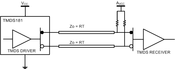 Figure 28. TMDS Driver and Termination Circuit
Referring to Figure 28, if VCC (TMDS181 supply) and AVCC (sink termination supply) are both powered, the TMDS output signals are high impedance when OE = high. The normal operating condition is that both supplies are active. Refer to Figure 28, if VCC is on and AVCC is off, the TMDS outputs source a typical 5-mA current through each termination resistor to ground. A total of 33 mW of power is consumed by the terminations independent of the OEB logical selection. When AVCC is powered on, normal operation (OE controls output impedance) is resumed. When the power source of the device is off and the power source to termination is on, the IO(off) output leakage current specification ensures the leakage current is limited to 45 μA or less. The VOD of the clock and data lanes can be reduced through I2C. See Table 12 for details. Figure 3 shows the different output voltages based on the different VSADJ settings.
8.3.11 Pre-Emphasis/De-Emphasis
The TMDS181 provides de-emphasis as a way to compensate for ISI loss between the TMDS181 outputs to a TMDS receiver. There are two methods to implement this function. When in pin strapping mode the PRE_SEL pin controls this function. The PRE_SEL pin provides - 2 dB or 0 dB de-emphasis, which allows the output signal pre-conditioning to offset interconnect losses from the TMDS181 device to the TMDS receiver. De-emphasis is recommended to be set at 0 dB while connecting to a receiver through short PCB route. When pulled to ground though a 65 kΩ resistor - 2 dB can be realized, see Figure 11. When using I2C, reg0Ch[1:0] is used to make these adjustments.
As there are times that true pre-emphasis may be the best solution there are two ways to accomplish this. If pin strapping is being used the best method is to reduce the VSADJ resistor value thus increasing the VOD swing and then pulling the PRE_SEL pin to ground using the 65 kΩ resistor, see Figure 29. If using I2C there are two methods to accomplish this. The first is similar to pin strapping by reducing the VSADJ resistor value and then implementing - 2 dB de-emphasis. The second method is to set reg0Ch[7:5] = 011 and set reg0Ch[1:0] = 01 which will accomplish the same pre-emphasis setting, see Figure 30.
NOTE
De-emphasis is only implement able during retimer mode. In redriver mode this function is not available.
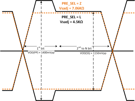 Figure 29. Output Pre-Emphasis Using Pin Strapping
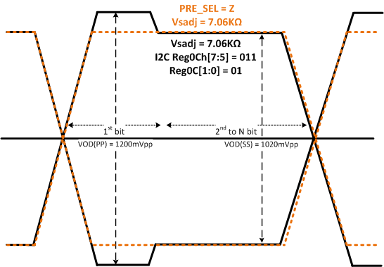 Figure 30. Output Pre-Emphasis Using I2C
8.4 Device Functional Modes
8.4.1 Retimer Mode
Clock and data recovery circuits (CDR) are used to track, sample, and retime the equalized data bit streams. The CDRs are designed with a loop bandwidth to minimize the amount of jitter transfer from the video source to the TMDS outputs. Input jitter within the CDR’s PLL bandwidth, < 1 MHz will be transferred to the TMDS outputs. Higher frequency jitter above the CDR loop bandwidth is attenuated, providing a jitter cleaning function to reduce the amount of high frequency jitter from the video source. The retimer is automatically activated at pixel clock approximately above 100 MHz when jitter cleaning is needed for robust operation when this option is enabled (default). The retimer operates at about 1 Gbps to 6 Gbps DR.
When systems switch to higher data rates above 3.4 Gbps, the CDR operates at between 85 MHz to 150 MHz pixel clock (3.4+ to 6.0 Gbps), supporting up to 4K2K high resolution with a 60 Hz refresh rate, or 3D 1080p HDTV. At pixel clock below 100 MHz, the TMDS181 automatically bypasses the internal retimer and operates as a redriver. When the video source changes resolution, the internal retimer starts the acquisition process to determine the input clock frequency and acquire lock to new data bit streams. During the clock frequency detection period and the retimer acquisition period that last approximately 7 ms, the TMDS drivers can be kept active (default) or programmed to be disabled to avoid sending invalid clock or data to the downstream receiver. The TMDS181 can be configured to work as a redriver (full range), crossover (redriver-retimer), and retimer (full range).
8.4.2 Redriver Mode
The TMDS181 also has a redriver mode that can be enabled through I2C, at reg0Ah[1:0] DEV_FUNC_MODE, which compensates for ISI channel loss. In this mode, power is reduced as the CDR and PLL are turned off. When in automatic mode, the TMDS181 is in redriver mode for data rates <1.0 Gbps. By using I2C, the device can be put in redriver mode for the complete data range of 250 Mbps to 3.4 Gbps. This is done by writing a 00 to register 0Ah[1:0]. If the link has excessive random jitter, then retimer mode is the best operating mode. When in redriver mode, the device only compensates for ISI loss. When in redriver mode compliance is not guaranteed as skew compensation and retiming functions are disabled. If a significant amount of random jitter is present, the system may not pass compliance at the connector.
8.4.3 DDC Training for HDMI2.0a Data Rate Monitor
As part of discovery, the source reads the sink’s E-EDID information to understand the capabilities of the sink. Part of this read is HDMI Forum Vendor Specific Data Block (HF-VSDB) MAX_TMDS_Character_Rate byte to determine the data rate supported. Depending upon the value, the source writes to slave address 0xA8 offset 0x20 bit1, TMDS_CLOCK_RATIO_STATUS. The TMDS181 snoops this write to determine the TMDS clock ratio and thus sets its own TMDS_CLOCK_RATIO_STATUS bit accordingly. If a 1 is written, then the TMDS clock is set to 1/40th of TMDS bit period. If a 0 is written, then the TMDS clock is set to 1/10th of TMDS bit period. The TMDS181 defaults to 1/10th of TMDS bit period unless a 1 is written to address 0xA8 offset 0x20 bit 1. When HPD is deasserted, this bit is reset to default values. If the source does not write this bit, the TMDS181 will not be configured for TMDS clock 1/40th mode in support of HDMI2.0a. As the TMDS181 is in the system link, but not recognized as part of the link, it is possible that the source could read the sink EDID where this bit is set and does not rewrite this bit. If the TMDS181 has entered a power-down state, this bit is cleared and does not re-set on a read. To work properly, the bit has to be set again with a write by the source.
8.4.4 DDC Functional Description
The TMDS181 solves sink/source level issues by implementing a master/slave control mode for the DDC bus. When the TMDS181 detects the start condition on the DDC bus from the SDA_SRC/SCL_SRC, it will transfer the data or clock signal to the SDA_SNK/SCL_SNK with little propagation delay. When SDA_SNK detects the feedback from the downstream device, the TMDS181 will pull up or pull down the SDA_SRC bus and deliver the signal to the source.
The DDC link defaults to 100 kbps but can be set to various values including 400 kbps by setting the correct value to address 0Bh through the I2C interface. The DDC lines are 5 V tolerant when the device is powered off.
NOTE
The TMDS181 utilizes clock stretching for DDC transactions. As there are sources and sinks that do not perform this function correctly a system may not work correctly as DDC transactions are incorrectly transmitted/received. To overcome this a snoop configuration can be implemented where the SDA/SCL from the source is connected directly to the SDA/SCL sink. The TMDS181 will need its SDA_SNK and SCL_SNK pins connected to this link in order to correctly configure the TMDS_CLOCK_RATIO_STATUS bit. Care must be taken when this configuration is being implemented as the voltage levels for DDC between the source and sink may be different, 3.3 V vs 5 V; See Figure 35 and See Figure 36
8.4.5 Mode Selection Functional Description
Mode selection definition: This bit lets the receiver know where the device is located in a system for the purpose of centering the AEQ point. The TMDS181 is targeting sink applications, so the default value is 1, which will center the EQ at 12 to 13 dB depending upon TMDS_CLOCK_RATIO_STATUS value (see Equalization Control Register). If the TMDS181 is in a source application, the value should be changed to a value of 0, which centers the EQ at 6.5 to 7.5 dB depending upon the TMDS_CLOCK_RATIO_STATUS value.
8.5 Register Maps
8.5.1 Local I2C Overview
The TMDS181 local I2C interface is always enabled, but will only be able to overwrite pin strapped features when I2C_EN/PIN is high. The SCL_CTL and SDA_CTL terminals are used for I2C clock and data respectively. The TMDS181 I2C interface conforms to the two-wire serial interface defined by the I2C Bus Specification, Version 2.1 (January 2000), and supports the fast mode transfer up to 400 kbps.
The device address byte is the first byte received following the START condition from the master device. The 7-bit device address for TMDS181 decides by the combination of EQ_SEL/A0 and A1. Figure 31 clarifies the TMDS181 target address.
| A1/A0 | 7 (MSB) | 6 | 5 | 4 | 3 | 2 | 1 | 0 (W/R) | HEX |
| 00 | 1 | 0 | 1 | 1 | 1 | 1 | 0 | 0/1 | BC/BD |
| 01 | 1 | 0 | 1 | 1 | 1 | 0 | 1 | 0/1 | BA/BB |
| 10 | 1 | 0 | 1 | 1 | 1 | 0 | 0 | 0/1 | B8/B9 |
| 11 | 1 | 0 | 1 | 1 | 0 | 1 | 1 | 0/1 | B6/B7 |
The typical source application of the TMDS181 is as a retimer in a TV connecting the HDMI output connector and an internal HDMI transmit through flat cables. The register setup can adjust by source side. When TMDS181 is used in a sink side application, it receives data from input connector and transmits to receiver. Local I2C buses run at 400 kHz supporting fast-mode I2C operation.
The following procedure is used to write to the TMDS181 I2C registers:
- The master initiates a write operation by generating a start condition (S), followed by the TMDS181 7-bit address and a zero-value W/R bit to indicate a write cycle.
- The TMDS181 acknowledges the address cycle.
- The master presents the sub-address (I2C register within TMDS181) to be written, consisting of one byte of data, MSB-first.
- The TMDS181 acknowledges the sub-address cycle.
- The master presents the first byte of data to be written to the I2C register.
- The TMDS181 acknowledges the byte transfer.
- The master may continue presenting additional bytes of data to be written, with each byte transfer completing with an acknowledge from the TMDS181.
- The master terminates the write operation by generating a stop condition (P).
The following procedure is used to read the TMDS181 I2C registers.
- The master initiates a read operation by generating a start condition (S), followed by the TMDS181 7-bit address and a one-value W/R bit to indicate a read cycle.
- The TMDS181 acknowledges the address cycle.
- The TMDS181 transmits the contents of the memory registers MSB-first starting at register 00h.
- The TMDS181 waits for either an acknowledge (ACK) or a not-acknowledge (NACK) from the master after each byte transfer; the I2C master acknowledges reception of each data byte transfer.
- If an ACK is received, the TMDS181 transmits the next byte of data.
- The master terminates the read operation by generating a stop condition (P).
NOTE
Upon reset, the TMDS181 sub-address is always set to 0x00. When no sub-address is included in a read operation, the TMDS181 sub-address increments from the previous acknowledged read or write data byte. If it is required to read from a sub-address that is different from the TMDS181 internal sub-address, a write operation with only a sub-address specified is needed before performing the read operation.
Refer to Local I2C Control Bit Access TAG Convention for TMDS181 local I2C register descriptions. Reads from reserved fields not described return zeros, and writes are ignored.
8.5.2 Local I2C Control Bit Access TAG Convention
Reads from reserved fields return zero, and writes to read-only reserved registers are ignored. All addresses not defined by this specification are considered reserved. Reads from these addresses return zero and writes are ignored.
BIT ACCESS TAG CONVENTIONS
A table of bit descriptions is typically included for each register description that indicates the bit field name, field description, and the field access tags. Table 4 describes the field access tags.
8.5.3 CSR Bit Field Definitions
8.5.3.1 ID Registers
Table 5. ID Registers Field Descriptions
| ADDRESS | BITS | DESCRIPTION | ACCESS |
|---|---|---|---|
| 00h~07h | 7:0 | DEVICE_ID These fields return a string of ASCII characters “TMDS181” followed by one space character. TMDS181: Address 0x00 – 0x07 = {- 0x54”T”, 0x4D”M”, 0x44”D”, 0x53”S”, 0x31”1”, 0x38”8”, 0x31”1”, 0x20}, |
R |
| 08h | 7:0 | REV _ID. This field identifies the device revision. 0000001 – TMDS181 revision 1 |
R |
8.5.3.2 MISC CONTROL Register
Table 6. MISC CONTROL Register Field Descriptions
| ADDRESS | BITS | DEFAULT | DESCRIPTION | ACCESS |
|---|---|---|---|---|
| 09h | 7 | 1’b0 | LANE_SWAP. This field swaps the input lanes as per Figure 26. 0 – Disable (default) no lane swap 1 – Enable: Swaps input lanes (redriver and retimer mode) Note: Field is loaded from SWAP/POL pin; Writes are ignored when I2C_EN/PIN = 0 |
RWU |
| 6 | 1’b0 | LANE_POLARITY swaps the input data and clock lanes polarity. 0 – Disabled (default) no polarity swap 1 – Swaps the input data and clock lane polarity (retimer mode only) Note: Field is loaded from SWAP/POL pin; Writes are ignored when I2C_EN/PIN = 0 |
RWU | |
| 5 | 1’b0 | Reserved | R | |
| 4 | 1’b0 | SIG_EN. This field enables the clock lane activity detect circuitry. (Redriver mode only because the retimer requires a clock input to work, so without a clock input, the device enters standby regardless) 0 – Disable (default) Clock detector circuit closed and receiver always works in normal operation. 1 – Enable, clock detector circuit makes the receiver automatically enter the standby state when no valid data detect. Note: Field is loaded from SIG_EN pin; Writes are ignored when I2C_EN/PIN = 0 |
RWU | |
| 3 | 1’b0 | PD_EN 0 – Normal working (default) 1 – Forced power down by I2C, lowest power state |
RW | |
| 2 | 1’b0 | HPD_AUTO_PWRDWN_DISABLE 0 – Automatically enters power-down mode based on HPD_SNK (default) 1 – Does not automatically enter power down mode |
RW | |
| 1:0 | 2’b10 | I2C_DR_CTL. I2C data rate supported for configuring device. 00 – 5 Kbps 01 – 10 Kbps 10 – 100 Kbps (default) 11 – 400 Kbps (Note: HPD_AUTO_PWRDWN_DISABLE must be set before enabling 400 Kbps mode) |
RW | |
| 0Ah | 7 | 1’b1 | Application mode selection (see Device Functional Modes) TMDS181 0 – Source 1 – Sink (default) |
RW |
| 6 | 1’b0 | HPDSNK_GATE_EN. The field sets the functional relationship between HPD_SNK and HPD_SRC. 0 – HPD_SNK passed through to the HPD_SRC (default) 1 – HPD_SNK does not pass through to the HPD_SRC. |
RW | |
| 5 | 1’b1 | EQ_ADA_EN. This field enables the equalizer functioning state. 0 – Fixed EQ 1 – Adaptive EQ (default) Writes are ignored when I2C_EN/PIN = 0 |
RWU | |
| 4 | 1’b1 | EQ_EN. This field enables the equalizer. 0 -- EQ disable 1 – EQ enable (default) Writes are ignored when I2C_EN/PIN = 0 |
RW | |
| 3 | 1’b0 | Reserved | R | |
| 2 | 1’b0 | APPLY_RXTX_CHANGES, Self-clearing write-only bit. Writing a 1 to this bit will apply new TX_TERM, HDMI_TWPST1, EQ_EN, EQ_ADA_EN, VSWING, Fixed EQ Value settings to the clock and data lanes. Writes to the respective registers do not take immediate effect. This bit does not need to be written if I2C configuration occurs while HPD_SNK are low, I2CPD_EN = 1 or there is no HDMI clock applied and SIGN_EN is high. |
W | |
| 1:0 | 2’b01 | DEV_FUNC_MODE. This field selects the device working function mode. 00 – Redriver mode: 250 Mbps – 3.4 Gbps 01 – Automatic redriver to retimer crossover at 1.0 Gbps (default) 10 – Automatic retimer when HDMI2.0a based upon TMDS_CLOCK_RATIO_STATUS 11 – Retimer mode across full range 250 Mbps to 6 Gbps When changing crossover point, need to toggle PD_EN or toggle external HPD_SNK. |
RW | |
| 0Bh | 7:5 | 3’b000 | Reserved | R |
| 4:3 | 2'b00 | TX_TERM_CTL. Controls termination for HDMI TX. 00 – No termination (default) 01 – 150 Ω to 300 Ω 10 – Reserved 11 – 75 Ω to 150 Ω Note: Writes are ignored when I2C_EN/PIN = 0; reflects the value of TX_TERM_CTL pin. |
RWU | |
| 2 | 1'b0 | DDC_DR_SEL Defines the DDC output speed for DDC bridge 0 = 100 kbps (default) 1 = 400 kbps (Note: HPD_AUTO_PWRDWN_DISABLE must be set before enabling 400 Kbps mode) |
RW | |
| 1 | 1'b0 | TMDS_CLOCK_RATIO_STATUS. This field is updated from snoop of DDC write to slave address 0xA8 offset 0x20 bit 1 that occurred on the SDA_SRC/SCL_SRC interface. When bit 1 of address 0xA8 offset 0x20 in the SCDC register set is written to a 1’b1, then this field will be set to a 1’b1. When bit 1 of address 0xA8 offset 0x20 is written to a 1’b0, then this field will be set to a 1’b0. This field is reset to default value whenever HPD_SNK is de-asserted for greater than 2 ms. 0 – TMDS Clock is 1/10 of TMDS bit period (default) 1 – TMDS Clock is 1/40 of TMDS bit period |
RWU | |
| 0 | 1'b0 | DDC_TRAIN_SETDISABLE; This field indicate the DDC training block function status. If disabled the device will only work in HDMI1.x or DVI modes. 0 – DDC training enable (default) 1 – DDC training disable Note: To force TMDS_CLOCK_RATIO_STATUS to 1 this register bit must be set to 1 which will force the 1/40 mode for HDMI2.0 |
RW | |
| 0Ch | 7:5 | 3’b000 | VSWING_DATA: Data output swing control 000 – Vsadj set (default) 001 – Increase by 7% 010 – Increase by 14% 011 – Increase by 21% 100 – Decrease by 30% 101 – Decrease by 21% 110 – Decrease by 14% 111 – Decrease by 7% |
RW |
| 4:2 | 3’b000 | VSWING_CLK: Clock output swing control: Default is set by Vsadj resistor value and the value of reg_0Dh[0]. 000 – Vsadj (default) 001 – Increase by 7% 010 – Increase by 14% 011 – Increase by 21% 100 – Decrease by 30% 101 – Decrease by 21% 110 – Decrease by 14% 111 – Decrease by 7% |
RW | |
| 1:0 | 2’b00 | HDMI_TWPST1[1:0]. HDMI de-emphasis FIR post-cursor-1 signed tap weight. (Retimer Mode Only) 00 – No de-emphasis (default) 01 – 2 dB de-emphasis 10 – Reserved 11 – Reserved Note: Reflects value of PRE_SEL pin; Writes are ignored when I2C_EN/PIN = 0 |
RWU |
8.5.3.3 Equalization Control Register
Table 7. Equalization Control Register Field Descriptions
| ADDRESS | BITS | DEFAULT | DESCRIPTION | ACCESS | |
|---|---|---|---|---|---|
| 0Dh | 7:6 | 2’b00 | Reserved | R | |
| 5:3 | 1’b000 | Data lane EQ – Sets fixed EQ values | RW | ||
| HDMI1.x | HDMI2.0a | ||||
| 000 – 0 dB (default) | 000 – 0 dB (default) | ||||
| 001 – 4.5 dB | 001 – 3 dB | ||||
| 010 – 6.5 dB | 010 – 5 dB | ||||
| 011 – 8.5 dB | 011 – 7.5 dB | ||||
| 100 – 10.5 dB | 100 – 9.5 dB | ||||
| 101 – 12 dB | 101 – 11 dB | ||||
| 110 – 14 dB | 110 – 13 dB | ||||
| 111 – 16.5 dB | 111 – 14.5 dB | ||||
| 2:1 | 1’b00 | Clock lane EQ - Sets fixed EQ values | RW | ||
| HDMI1.x | HDMI2.0a | ||||
| 00 – 0 dB (default) | 00 – 0 dB (default) | ||||
| 01 – 1.5 dB | 01 – 1.5 dB | ||||
| 10 – 3 dB | 10 – 3 dB | ||||
| 11 – RSVD | 11 – 4.5 dB | ||||
| 0 | 1’b0 | DIS_HDMI2_SWG: 0 – Clock VOD is half of set values when TMDS_CLOCK_RATIO_STATUS states in HDMI2.0a mode (default) 1 – Disables TMDS_CLOCK_RATIO_STATUS control of the clock VOD so output swing is at full swing. |
RW | ||