SBOS231I January 2002 – November 2015 TMP100 , TMP101
PRODUCTION DATA.
- 1 Features
- 2 Applications
- 3 Description
- 4 Revision History
- 5 Pin Configuration and Functions
- 6 Specifications
-
7 Detailed Description
- 7.1 Overview
- 7.2 Functional Block Diagram
- 7.3 Feature Description
- 7.4 Device Functional Modes
- 7.5 Programming
- 8 Application and Implementation
- 9 Power Supply Recommendations
- 10Layout
- 11Device and Documentation Support
- 12Mechanical, Packaging, and Orderable Information
Package Options
Mechanical Data (Package|Pins)
- DBV|6
Thermal pad, mechanical data (Package|Pins)
Orderable Information
8 Application and Implementation
NOTE
Information in the following applications sections is not part of the TI component specification, and TI does not warrant its accuracy or completeness. TI’s customers are responsible for determining suitability of components for their purposes. Customers should validate and test their design implementation to confirm system functionality.
8.1 Application Information
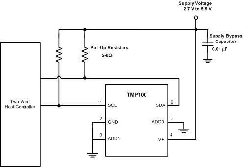
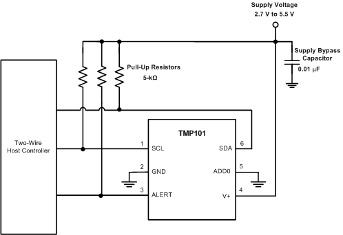
The TMP100 and TMP101 devices are used to measure the printed circuit board (PCB) temperature of the board location where the devices are mounted. The TMP100 features two address pins to allow up to eight devices to be addressed on a single I2C interface. The TMP101 device features one address pin and an ALERT pin, allowing up to three devices to be connected per bus. The TMP100 and TMP101 devices require no external components for operation except for pullup resistors on SCL, SDA, and ALERT (TMP101 device), although a 0.1-μF bypass capacitor is recommended.
The sensing device of the TMP100 and TMP101 devices is the chip itself. Thermal paths run through the package leads as well as the plastic package. The die flag of the lead frame is connected to GND. The lower thermal resistance of metal causes the leads to provide the primary thermal path. The GND pin of the TMP100 or TMP101 device is directly connected to the metal lead frame, and is the best choice for thermal input.
8.2 Typical Application
 Figure 12. Typical Connections of the TMP100
 Figure 13. Typical Connections of the TMP101
8.2.1 Design Requirements
The TMP100 and TMP101 devices require pullup resistors on the SCL, SDA, and ALERT (TMP101 device) pins. The recommended value for the pullup resistor is 5-kΩ. In some applications, the pullup resistor can be lower or higher than 5-kΩ but must not exceed 3 mA of current on the SCL and SDA pins, and must not exceed 4 mA on the ALERT (TMP101) pin. A 0.1-μF bypass capacitor is recommended, as shown in Figure 12 and Figure 13. The SCL, SDA, and ALERT lines can be pulled up to a supply that is equal to or higher than VS through the pullup resistors. For the TMP100, to configure one of eight different addresses on the bus, connect ADD0 and ADD1 to either the GND pin, V+ pin, or float. Float indicates the pin is left unconnected. For the TMP101 device, to configure one of three different addresses on the bus, connect ADD0 to either the GND pin, V+ pin, or float.
8.2.2 Detailed Design Procedure
Place the TMP100 and TMP101 devices in close proximity to the heat source that must be monitored, with a proper layout for good thermal coupling. This placement ensures that temperature changes are captured within the shortest possible time interval. To maintain accuracy in applications that require air or surface temperature measurement, care must be taken to isolate the package and leads from ambient air temperature. A thermally-conductive adhesive is helpful in achieving accurate surface temperature measurement.
8.2.3 Application Curve
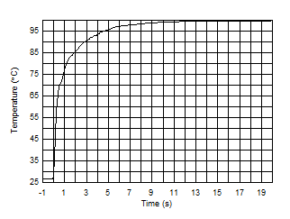
Figure 14 shows the step response of the TMP100 and TMP101 devices to a submersion in an oil bath of 100ºC from room temperature (27ºC). The time constant, or the time for the output to reach 63% of the input step, is
0.9 s. The time-constant result depends on the PCB that the TMP100 and TMP101 devices are mounted. For this test, the TMP100 and TMP101 devices are soldered to a two-layer PCB that measures 0.375 inch × 0.437 inch.
 Figure 14. Temperature Step Response