SBOS231I January   2002  – November 2015 TMP100 , TMP101

PRODUCTION DATA.  

  1. Features
  2. Applications
  3. Description
  4. Revision History
  5. Pin Configuration and Functions
  6. Specifications
    1. 6.1 Absolute Maximum Ratings
    2. 6.2 ESD Ratings
    3. 6.3 Recommended Operating Conditions
    4. 6.4 Thermal Information
    5. 6.5 Electrical Characteristics
    6. 6.6 Timing Requirements
    7. 6.7 Typical Characteristics
  7. Detailed Description
    1. 7.1 Overview
    2. 7.2 Functional Block Diagram
    3. 7.3 Feature Description
      1. 7.3.1 Digital Temperature Output
      2. 7.3.2 Serial Interface
        1. 7.3.2.1 Bus Overview
        2. 7.3.2.2 Serial Bus Address
        3. 7.3.2.3 Writing and Reading to the TMP100 and TMP101
        4. 7.3.2.4 Slave Mode Operations
          1. 7.3.2.4.1 Slave Receiver Mode
          2. 7.3.2.4.2 Slave Transmitter Mode
        5. 7.3.2.5 SMBus Alert Function
        6. 7.3.2.6 General Call
        7. 7.3.2.7 High-Speed Mode
        8. 7.3.2.8 POR (Power-On Reset)
      3. 7.3.3 Timing Diagrams
    4. 7.4 Device Functional Modes
      1. 7.4.1 Shutdown Mode (SD)
      2. 7.4.2 OS/ALERT (OS)
      3. 7.4.3 Thermostat Mode (TM)
        1. 7.4.3.1 Comparator Mode (TM = 0)
        2. 7.4.3.2 Interrupt Mode (TM = 1)
    5. 7.5 Programming
      1. 7.5.1 Pointer Register
        1. 7.5.1.1 Pointer Register Byte (pointer = N/A) [reset = 00h]
        2. 7.5.1.2 Pointer Addresses of the TMP100 and TMP101 Registers
      2. 7.5.2 Temperature Register
      3. 7.5.3 Configuration Register
        1. 7.5.3.1 Shutdown Mode (SD)
        2. 7.5.3.2 Thermostat Mode (TM)
        3. 7.5.3.3 Polarity (POL)
        4. 7.5.3.4 Fault Queue (F1, F0)
        5. 7.5.3.5 Converter Resolution (R1, R0)
        6. 7.5.3.6 OS/ALERT (OS)
      4. 7.5.4 High- and Low-Limit Registers
  8. Application and Implementation
    1. 8.1 Application Information
    2. 8.2 Typical Application
      1. 8.2.1 Design Requirements
      2. 8.2.2 Detailed Design Procedure
      3. 8.2.3 Application Curve
  9. Power Supply Recommendations
  10. 10Layout
    1. 10.1 Layout Guidelines
    2. 10.2 Layout Examples
  11. 11Device and Documentation Support
    1. 11.1 Related Links
    2. 11.2 Trademarks
    3. 11.3 Electrostatic Discharge Caution
    4. 11.4 Glossary
  12. 12Mechanical, Packaging, and Orderable Information

Package Options

Mechanical Data (Package|Pins)
Thermal pad, mechanical data (Package|Pins)
Orderable Information

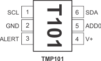
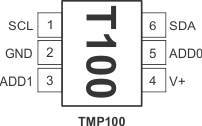
5 Pin Configuration and Functions

DBV Package
6-Pin SOT-23
Top View
TMP100 TMP101 pin_1_config_sbos231.gif
DBV Package
6-Pin SOT-23
Top View
TMP100 TMP101 pin_2_config_sbos231.gif

Pin Functions

PIN I/O DESCRIPTION
NAME NO.
TMP100 TMP101
ADD0 5 5 I Address select. Connect to GND, V+, or leave floating.
ADD1 3 I Address select. Connect to GND, V+, or leave floating.
ALERT 3 O Overtemperature alert. Open-drain output; requires a pullup resistor.
GND 2 2 Ground
SCL 1 1 I Serial clock. Open-drain output; requires a pullup resistor.
SDA 6 6 I/O Serial data. Open-drain output; requires a pullup resistor.
V+ 4 4 I Supply voltage, 2.7 V to 5.5 V