SBOS288M January   2004  – December 2020 TMP175 , TMP75

PRODUCTION DATA  

  1. Features
  2. Applications
  3. Description
  4. Revision History
  5. Pin Configuration and Functions
  6. Specifications
    1. 6.1 Absolute Maximum Ratings
    2. 6.2 ESD Ratings
    3. 6.3 Recommended Operating Conditions
    4. 6.4 Thermal Information
    5. 6.5 Electrical Characteristics
    6. 6.6 I2C Interface Timing
    7. 6.7 Typical Characteristics
  7. Detailed Description
    1. 7.1 Overview
    2. 7.2 Functional Block Diagram
    3. 7.3 Feature Description
      1. 7.3.1 Digital Temperature Output
      2. 7.3.2 Serial Interface
        1. 7.3.2.1 Bus Overview
        2. 7.3.2.2 Serial Bus Address
        3. 7.3.2.3 Writing and Reading to the TMP175 and TMP75
        4. 7.3.2.4 Slave Mode Operations
          1. 7.3.2.4.1 Slave Receiver Mode
          2. 7.3.2.4.2 Slave Transmitter Mode
        5. 7.3.2.5 SMBus Alert Function
        6. 7.3.2.6 General Call
        7. 7.3.2.7 High-Speed Mode
        8. 7.3.2.8 Time-out Function
      3. 7.3.3 Timing Diagrams
      4. 7.3.4 Two-Wire Timing Diagrams
    4. 7.4 Device Functional Modes
      1. 7.4.1 Shutdown Mode (SD)
      2. 7.4.2 One-shot (OS)
      3. 7.4.3 Thermostat Mode (TM)
      4. 7.4.4 Comparator Mode (TM = 0)
      5. 7.4.5 Interrupt Mode (TM = 1)
    5. 7.5 Programming
      1. 7.5.1 Pointer Register
        1. 7.5.1.1 Pointer Register Byte (pointer = N/A) [reset = 00h]
        2. 7.5.1.2 Pointer Addresses of the TMP175
      2. 7.5.2 Temperature Register
      3. 7.5.3 Configuration Register
        1. 7.5.3.1 Shutdown Mode (SD)
        2. 7.5.3.2 Thermostat Mode (TM)
        3. 7.5.3.3 Polarity (POL)
        4. 7.5.3.4 Fault Queue (F1/F0)
        5. 7.5.3.5 Converter Resolution (R1/R0)
        6. 7.5.3.6 One-Shot (OS)
      4. 7.5.4 High and Low Limit Registers
  8. Application and Implementation
    1. 8.1 Application Information
    2. 8.2 Typical Application
      1. 8.2.1 Design Requirements
      2. 8.2.2 Detailed Design Procedure
      3. 8.2.3 Application Curve
  9. Power Supply Recommendations
  10. 10Layout
    1. 10.1 Layout Guidelines
    2. 10.2 Layout Example
  11. 11Device and Documentation Support
    1. 11.1 Receiving Notification of Documentation Updates
    2. 11.2 Support Resources
    3. 11.3 Trademarks
    4. 11.4 Electrostatic Discharge Caution
    5. 11.5 Glossary
  12. 12Mechanical, Packaging, and Orderable Information

Package Options

Mechanical Data (Package|Pins)
Thermal pad, mechanical data (Package|Pins)
Orderable Information

Polarity (POL)

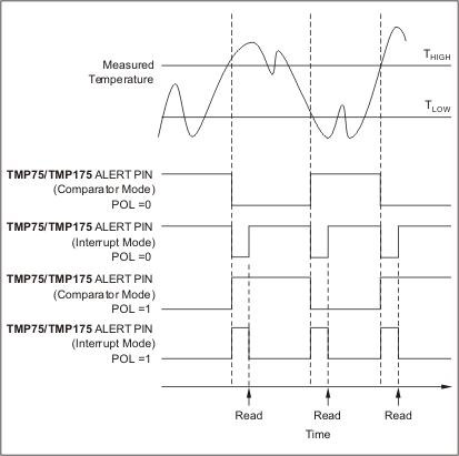
The polarity bit of the TMP175 lets the user adjust the polarity of the ALERT pin output. If the POL bit is set to 0 (default), the ALERT pin becomes active low. When POL bit is set to 1, the ALERT pin becomes active high and the state of the ALERT pin is inverted. The operation of the ALERT pin in various modes is illustrated in Figure 7-7.
GUID-883D48C4-AFB5-420E-8B31-FE9D27A890A8-low.gifFigure 7-7 Output Transfer Function Diagrams