SPRS945G January   2017  – January 2023 TMS320F280040-Q1 , TMS320F280040C-Q1 , TMS320F280041 , TMS320F280041-Q1 , TMS320F280041C , TMS320F280041C-Q1 , TMS320F280045 , TMS320F280048-Q1 , TMS320F280048C-Q1 , TMS320F280049 , TMS320F280049-Q1 , TMS320F280049C , TMS320F280049C-Q1

PRODUCTION DATA  

  1. Features
  2. Applications
  3. Description
    1. 3.1 Functional Block Diagram
  4. Revision History
  5. Device Comparison
    1. 5.1 Related Products
  6. Pin Configuration and Functions
    1. 6.1 Pin Diagrams
    2. 6.2 Pin Attributes
    3. 6.3 Signal Descriptions
      1. 6.3.1 Analog Signals
      2. 6.3.2 Digital Signals
      3. 6.3.3 Power and Ground
      4. 6.3.4 Test, JTAG, and Reset
    4. 6.4 Pin Multiplexing
      1. 6.4.1 GPIO Muxed Pins
      2. 6.4.2 Digital Inputs on ADC Pins (AIOs)
      3. 6.4.3 GPIO Input X-BAR
      4. 6.4.4 GPIO Output X-BAR and ePWM X-BAR
    5. 6.5 Pins With Internal Pullup and Pulldown
    6. 6.6 Connections for Unused Pins
  7. Specifications
    1. 7.1  Absolute Maximum Ratings
    2. 7.2  ESD Ratings – Commercial
    3. 7.3  ESD Ratings – Automotive
    4. 7.4  Recommended Operating Conditions
    5. 7.5  Power Consumption Summary
      1. 7.5.1 System Current Consumption (External Supply)
      2. 7.5.2 System Current Consumption (Internal VREG)
      3. 7.5.3 System Current Consumption (DCDC)
      4. 7.5.4 Operating Mode Test Description
      5. 7.5.5 Current Consumption Graphs
      6. 7.5.6 Reducing Current Consumption
        1. 7.5.6.1 Typical IDD Current Reduction per Disabled Peripheral (at 100-MHz SYSCLK)
    6. 7.6  Electrical Characteristics
    7. 7.7  Thermal Resistance Characteristics
      1. 7.7.1 PZ Package
      2. 7.7.2 PM Package
      3. 7.7.3 RSH Package
    8. 7.8  Thermal Design Considerations
    9. 7.9  System
      1. 7.9.1 Power Management Module (PMM)
        1. 7.9.1.1 Introduction
        2. 7.9.1.2 Overview
          1. 7.9.1.2.1 Power Rail Monitors
            1. 7.9.1.2.1.1 I/O POR (Power-On Reset) Monitor
            2. 7.9.1.2.1.2 I/O BOR (Brown-Out Reset) Monitor
            3. 7.9.1.2.1.3 VDD POR (Power-On Reset) Monitor
          2. 7.9.1.2.2 External Supervisor Usage
          3. 7.9.1.2.3 Delay Blocks
          4. 7.9.1.2.4 Internal 1.2-V LDO Voltage Regulator (VREG)
          5. 7.9.1.2.5 VREGENZ
          6. 7.9.1.2.6 Internal 1.2-V Switching Regulator (DC-DC)
            1. 7.9.1.2.6.1 PCB Layout and Component Guidelines
        3. 7.9.1.3 External Components
          1. 7.9.1.3.1 Decoupling Capacitors
            1. 7.9.1.3.1.1 VDDIO Decoupling
            2. 7.9.1.3.1.2 VDD Decoupling
        4. 7.9.1.4 Power Sequencing
          1. 7.9.1.4.1 Supply Pins Ganging
          2. 7.9.1.4.2 Signal Pins Power Sequence
          3. 7.9.1.4.3 Supply Pins Power Sequence
            1. 7.9.1.4.3.1 External VREG/VDD Mode Sequence
            2. 7.9.1.4.3.2 Internal VREG/VDD Mode Sequence
            3. 7.9.1.4.3.3 Supply Sequencing Summary and Effects of Violations
            4. 7.9.1.4.3.4 Supply Slew Rate
        5. 7.9.1.5 Power Management Module Electrical Data and Timing
          1. 7.9.1.5.1 Power Management Module Operating Conditions
          2. 7.9.1.5.2 Power Management Module Characteristics
          3.        Supply Voltages
      2. 7.9.2 Reset Timing
        1. 7.9.2.1 Reset Sources
        2. 7.9.2.2 Reset Electrical Data and Timing
          1. 7.9.2.2.1 Reset (XRSn) Timing Requirements
          2. 7.9.2.2.2 Reset (XRSn) Switching Characteristics
          3. 7.9.2.2.3 Reset Timing Diagram
      3. 7.9.3 Clock Specifications
        1. 7.9.3.1 Clock Sources
        2. 7.9.3.2 Clock Frequencies, Requirements, and Characteristics
          1. 7.9.3.2.1 Input Clock Frequency and Timing Requirements, PLL Lock Times
            1. 7.9.3.2.1.1 Input Clock Frequency
            2. 7.9.3.2.1.2 XTAL Oscillator Characteristics
            3. 7.9.3.2.1.3 X1 Timing Requirements
            4. 7.9.3.2.1.4 PLL Lock Times
          2. 7.9.3.2.2 Internal Clock Frequencies
            1. 7.9.3.2.2.1 Internal Clock Frequencies
          3. 7.9.3.2.3 Output Clock Frequency and Switching Characteristics
            1. 7.9.3.2.3.1 XCLKOUT Switching Characteristics
        3. 7.9.3.3 Input Clocks and PLLs
        4. 7.9.3.4 Crystal (XTAL) Oscillator
          1. 7.9.3.4.1 Introduction
          2. 7.9.3.4.2 Overview
            1. 7.9.3.4.2.1 Electrical Oscillator
              1. 7.9.3.4.2.1.1 Modes of Operation
                1. 7.9.3.4.2.1.1.1 Crystal Mode of Operation
                2. 7.9.3.4.2.1.1.2 Single-Ended Mode of Operation
              2. 7.9.3.4.2.1.2 XTAL Output on XCLKOUT
            2. 7.9.3.4.2.2 Quartz Crystal
            3. 7.9.3.4.2.3 GPIO Modes of Operation
          3. 7.9.3.4.3 Functional Operation
            1. 7.9.3.4.3.1 ESR – Effective Series Resistance
            2. 7.9.3.4.3.2 Rneg – Negative Resistance
            3. 7.9.3.4.3.3 Start-up Time
            4. 7.9.3.4.3.4 DL – Drive Level
          4. 7.9.3.4.4 How to Choose a Crystal
          5. 7.9.3.4.5 Testing
          6. 7.9.3.4.6 Common Problems and Debug Tips
          7. 7.9.3.4.7 Crystal Oscillator Specifications
            1. 7.9.3.4.7.1 Crystal Oscillator Parameters
            2. 7.9.3.4.7.2 Crystal Equivalent Series Resistance (ESR) Requirements
            3. 7.9.3.4.7.3 Crystal Oscillator Electrical Characteristics
        5. 7.9.3.5 Internal Oscillators
          1. 7.9.3.5.1 INTOSC Characteristics
      4. 7.9.4 Flash Parameters
      5. 7.9.5 Emulation/JTAG
        1. 7.9.5.1 JTAG Electrical Data and Timing
          1. 7.9.5.1.1 JTAG Timing Requirements
          2. 7.9.5.1.2 JTAG Switching Characteristics
          3. 7.9.5.1.3 JTAG Timing Diagram
        2. 7.9.5.2 cJTAG Electrical Data and Timing
          1. 7.9.5.2.1 cJTAG Timing Requirements
          2. 7.9.5.2.2 cJTAG Switching Characteristics
          3. 7.9.5.2.3 cJTAG Timing Diagram
      6. 7.9.6 GPIO Electrical Data and Timing
        1. 7.9.6.1 GPIO – Output Timing
          1. 7.9.6.1.1 General-Purpose Output Switching Characteristics
        2. 7.9.6.2 GPIO – Input Timing
          1. 7.9.6.2.1 General-Purpose Input Timing Requirements
        3. 7.9.6.3 Sampling Window Width for Input Signals
      7. 7.9.7 Interrupts
        1. 7.9.7.1 External Interrupt (XINT) Electrical Data and Timing
          1. 7.9.7.1.1 External Interrupt Timing Requirements
          2. 7.9.7.1.2 External Interrupt Switching Characteristics
          3. 7.9.7.1.3 Interrupt Timing Diagram
      8. 7.9.8 Low-Power Modes
        1. 7.9.8.1 Clock-Gating Low-Power Modes
        2. 7.9.8.2 Low-Power Mode Wake-up Timing
          1. 7.9.8.2.1 IDLE Mode Timing Requirements
          2. 7.9.8.2.2 IDLE Mode Switching Characteristics
          3. 7.9.8.2.3 IDLE Mode Timing Diagram
          4. 7.9.8.2.4 HALT Mode Timing Requirements
          5. 7.9.8.2.5 HALT Mode Switching Characteristics
          6. 7.9.8.2.6 HALT Mode Timing Diagram
    10. 7.10 Analog Peripherals
      1. 7.10.1 Analog-to-Digital Converter (ADC)
        1. 7.10.1.1 Result Register Mapping
        2. 7.10.1.2 ADC Configurability
          1. 7.10.1.2.1 Signal Mode
        3. 7.10.1.3 ADC Electrical Data and Timing
          1. 7.10.1.3.1 ADC Operating Conditions
          2. 7.10.1.3.2 ADC Characteristics
          3. 7.10.1.3.3 ADC Input Model
          4. 7.10.1.3.4 ADC Timing Diagrams
      2. 7.10.2 Programmable Gain Amplifier (PGA)
        1. 7.10.2.1 PGA Electrical Data and Timing
          1. 7.10.2.1.1 PGA Operating Conditions
          2. 7.10.2.1.2 PGA Characteristics
          3. 7.10.2.1.3 PGA Typical Characteristics Graphs
      3. 7.10.3 Temperature Sensor
        1. 7.10.3.1 Temperature Sensor Electrical Data and Timing
          1. 7.10.3.1.1 Temperature Sensor Characteristics
      4. 7.10.4 Buffered Digital-to-Analog Converter (DAC)
        1. 7.10.4.1 Buffered DAC Electrical Data and Timing
          1. 7.10.4.1.1 Buffered DAC Operating Conditions
          2. 7.10.4.1.2 Buffered DAC Electrical Characteristics
          3. 7.10.4.1.3 Buffered DAC Illustrative Graphs
          4. 7.10.4.1.4 Buffered DAC Typical Characteristics Graphs
      5. 7.10.5 Comparator Subsystem (CMPSS)
        1. 7.10.5.1 CMPSS Electrical Data and Timing
          1. 7.10.5.1.1 Comparator Electrical Characteristics
          2. 7.10.5.1.2 CMPSS DAC Static Electrical Characteristics
          3. 7.10.5.1.3 CMPSS Illustrative Graphs
    11. 7.11 Control Peripherals
      1. 7.11.1 Enhanced Capture (eCAP)
        1. 7.11.1.1 eCAP Electrical Data and Timing
          1. 7.11.1.1.1 eCAP Timing Requirements
          2. 7.11.1.1.2 eCAP Switching Characteristics
      2. 7.11.2 High-Resolution Capture Submodule (HRCAP6–HRCAP7)
        1. 7.11.2.1 HRCAP Electrical Data and Timing
          1. 7.11.2.1.1 HRCAP Switching Characteristics
      3. 7.11.3 Enhanced Pulse Width Modulator (ePWM)
        1. 7.11.3.1 Control Peripherals Synchronization
        2. 7.11.3.2 ePWM Electrical Data and Timing
          1. 7.11.3.2.1 ePWM Timing Requirements
          2. 7.11.3.2.2 ePWM Switching Characteristics
          3. 7.11.3.2.3 Trip-Zone Input Timing
            1. 7.11.3.2.3.1 Trip-Zone Input Timing Requirements
        3. 7.11.3.3 External ADC Start-of-Conversion Electrical Data and Timing
          1. 7.11.3.3.1 External ADC Start-of-Conversion Switching Characteristics
      4. 7.11.4 High-Resolution Pulse Width Modulator (HRPWM)
        1. 7.11.4.1 HRPWM Electrical Data and Timing
          1. 7.11.4.1.1 High-Resolution PWM Characteristics
      5. 7.11.5 Enhanced Quadrature Encoder Pulse (eQEP)
        1. 7.11.5.1 eQEP Electrical Data and Timing
          1. 7.11.5.1.1 eQEP Timing Requirements
          2. 7.11.5.1.2 eQEP Switching Characteristics
      6. 7.11.6 Sigma-Delta Filter Module (SDFM)
        1. 7.11.6.1 SDFM Electrical Data and Timing
          1. 7.11.6.1.1 SDFM Timing Requirements When Using Asynchronous GPIO (ASYNC) Option
          2. 7.11.6.1.2 SDFM Timing Diagram
        2. 7.11.6.2 SDFM Electrical Data and Timing (Synchronized GPIO)
          1. 7.11.6.2.1 SDFM Timing Requirements When Using Synchronized GPIO (SYNC) Option
    12. 7.12 Communications Peripherals
      1. 7.12.1 Controller Area Network (CAN)
      2. 7.12.2 Inter-Integrated Circuit (I2C)
        1. 7.12.2.1 I2C Electrical Data and Timing
          1. 7.12.2.1.1 I2C Timing Requirements
          2. 7.12.2.1.2 I2C Switching Characteristics
          3. 7.12.2.1.3 I2C Timing Diagram
      3. 7.12.3 Power Management Bus (PMBus) Interface
        1. 7.12.3.1 PMBus Electrical Data and Timing
          1. 7.12.3.1.1 PMBus Electrical Characteristics
          2. 7.12.3.1.2 PMBus Fast Mode Switching Characteristics
          3. 7.12.3.1.3 PMBus Standard Mode Switching Characteristics
      4. 7.12.4 Serial Communications Interface (SCI)
      5. 7.12.5 Serial Peripheral Interface (SPI)
        1. 7.12.5.1 SPI Electrical Data and Timing
          1. 7.12.5.1.1 Non-High-Speed Master Mode Timings
            1. 7.12.5.1.1.1 SPI Master Mode Switching Characteristics (Clock Phase = 0)
            2. 7.12.5.1.1.2 SPI Master Mode Switching Characteristics (Clock Phase = 1)
            3. 7.12.5.1.1.3 SPI Master Mode Timing Requirements
          2. 7.12.5.1.2 Non-High-Speed Slave Mode Timings
            1. 7.12.5.1.2.1 SPI Slave Mode Switching Characteristics
            2. 7.12.5.1.2.2 SPI Slave Mode Timing Requirements
          3. 7.12.5.1.3 High-Speed Master Mode Timings
            1. 7.12.5.1.3.1 SPI High-Speed Master Mode Switching Characteristics (Clock Phase = 0)
            2. 7.12.5.1.3.2 SPI High-Speed Master Mode Switching Characteristics (Clock Phase = 1)
            3. 7.12.5.1.3.3 SPI High-Speed Master Mode Timing Requirements
          4. 7.12.5.1.4 High-Speed Slave Mode Timings
            1. 7.12.5.1.4.1 SPI High-Speed Slave Mode Switching Characteristics
            2. 7.12.5.1.4.2 SPI High-Speed Slave Mode Timing Requirements
      6. 7.12.6 Local Interconnect Network (LIN)
      7. 7.12.7 Fast Serial Interface (FSI)
        1. 7.12.7.1 FSI Transmitter
          1. 7.12.7.1.1 FSITX Electrical Data and Timing
            1. 7.12.7.1.1.1 FSITX Switching Characteristics
        2. 7.12.7.2 FSI Receiver
          1. 7.12.7.2.1 FSIRX Electrical Data and Timing
            1. 7.12.7.2.1.1 FSIRX Switching Characteristics
            2. 7.12.7.2.1.2 FSIRX Timing Requirements
        3. 7.12.7.3 FSI SPI Compatibility Mode
          1. 7.12.7.3.1 FSITX SPI Signaling Mode Electrical Data and Timing
            1. 7.12.7.3.1.1 FSITX SPI Signaling Mode Switching Characteristics
  8. Detailed Description
    1. 8.1  Overview
    2. 8.2  Functional Block Diagram
    3. 8.3  Memory
      1. 8.3.1 C28x Memory Map
      2. 8.3.2 Control Law Accelerator (CLA) ROM Memory Map
      3. 8.3.3 Flash Memory Map
      4. 8.3.4 Peripheral Registers Memory Map
      5. 8.3.5 Memory Types
        1. 8.3.5.1 Dedicated RAM (Mx RAM)
        2. 8.3.5.2 Local Shared RAM (LSx RAM)
        3. 8.3.5.3 Global Shared RAM (GSx RAM)
        4. 8.3.5.4 CLA Message RAM (CLA MSGRAM)
    4. 8.4  Identification
    5. 8.5  Bus Architecture – Peripheral Connectivity
    6. 8.6  C28x Processor
      1. 8.6.1 Embedded Real-Time Analysis and Diagnostic (ERAD)
      2. 8.6.2 Floating-Point Unit (FPU)
      3. 8.6.3 Trigonometric Math Unit (TMU)
      4. 8.6.4 Viterbi, Complex Math and CRC Unit (VCU-I)
    7. 8.7  Control Law Accelerator (CLA)
    8. 8.8  Direct Memory Access (DMA)
    9. 8.9  Boot ROM and Peripheral Booting
      1. 8.9.1 Configuring Alternate Boot Mode Select Pins
      2. 8.9.2 Configuring Alternate Boot Mode Options
      3. 8.9.3 GPIO Assignments
    10. 8.10 Dual Code Security Module
    11. 8.11 Watchdog
    12. 8.12 Configurable Logic Block (CLB)
    13. 8.13 Functional Safety
  9. Applications, Implementation, and Layout
    1. 9.1 Key Device Features
    2. 9.2 Application Information
      1. 9.2.1 Typical Application
        1. 9.2.1.1 Server Telecom Power Supply Unit (PSU)
          1. 9.2.1.1.1 System Block Diagram
          2. 9.2.1.1.2 Server and Telecom PSU Resources
        2. 9.2.1.2 Single-Phase Online UPS
          1. 9.2.1.2.1 System Block Diagram
          2. 9.2.1.2.2 Single phase online UPS Resources
        3. 9.2.1.3 Solar Micro Inverter
          1. 9.2.1.3.1 System Block Diagram
          2. 9.2.1.3.2 Solar Micro Inverter Resources
        4. 9.2.1.4 EV Charging Station Power Module
          1. 9.2.1.4.1 System Block Diagram
          2. 9.2.1.4.2 EV charging station power module Resources
        5. 9.2.1.5 Servo Drive Control Module
          1. 9.2.1.5.1 System Block Diagram
          2. 9.2.1.5.2 Servo Drive Control Module Resources
  10. 10Device and Documentation Support
    1. 10.1 Device and Development Support Tool Nomenclature
    2. 10.2 Markings
    3. 10.3 Tools and Software
    4. 10.4 Documentation Support
    5. 10.5 Support Resources
    6. 10.6 Trademarks
    7. 10.7 Electrostatic Discharge Caution
    8. 10.8 Glossary
  11. 11Mechanical, Packaging, and Orderable Information
    1. 11.1 Packaging Information

Package Options

Mechanical Data (Package|Pins)
Thermal pad, mechanical data (Package|Pins)
Orderable Information

Local Interconnect Network (LIN)

This device contains one Local Interconnect Network (LIN) module. The LIN module adheres to the LIN 2.1 standard as defined by the LIN Specification Package Revision 2.1. The LIN is a low-cost serial interface designed for applications where the CAN protocol may be too expensive to implement, such as small subnetworks for cabin comfort functions like interior lighting or window control in an automotive application.

The LIN standard is based on the SCI (UART) serial data link format. The communication concept is single-master and multiple-slave with a message identification for multicast transmission between any network nodes.

The LIN module can be programmed to work either as an SCI or as a LIN as the core of the module is an SCI. The hardware features of the SCI are augmented to achieve LIN compatibility. The SCI module is a universal asynchronous receiver-transmitter (UART) that implements the standard non-return-to-zero format.

Though the registers are common for LIN and SCI, the register descriptions have notes to identify the register/bit usage in different modes. Because of this, code written for this module cannot be directly ported to the stand-alone SCI module and vice versa.

The LIN module has the following features:

  • Compatibility with LIN 1.3, 2.0 and 2.1 protocols
  • Configurable baud rate up to 20 kbps (as per LIN 2.1 protocol)
  • Two external pins: LINRX and LINTX
  • Multibuffered receive and transmit units
  • Identification masks for message filtering
  • Automatic master header generation
    • Programmable synchronization break field
    • Synchronization field
    • Identifier field
  • Slave automatic synchronization
    • Synchronization break detection
    • Optional baud rate update
    • Synchronization validation
  • 231 programmable transmission rates with 7 fractional bits
  • Wakeup on LINRX dominant level from transceiver
  • Automatic wakeup support
    • Wakeup signal generation
    • Expiration times on wakeup signals
  • Automatic bus idle detection
  • Error detection
    • Bit error
    • Bus error
    • No-response error
    • Checksum error
    • Synchronization field error
    • Parity error
  • Capability to use direct memory access (DMA) for transmit and receive data
  • Two interrupt lines with priority encoding for:
    • Receive
    • Transmit
    • ID, error, and status
  • Support for LIN 2.0 checksum
  • Enhanced synchronizer finite state machine (FSM) support for frame processing
  • Enhanced handling of extended frames
  • Enhanced baud rate generator
  • Update wakeup/go to sleep

Figure 7-92 shows the LIN block diagram.
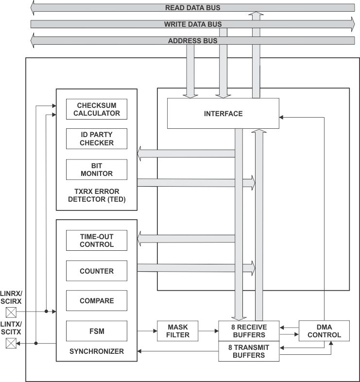
GUID-3A769FF8-69A2-4E60-9A7F-45ABAF357B55-low.gifFigure 7-92 LIN Block Diagram