SCDS419D November 2020 – January 2022 TMUX6208 , TMUX6209
PRODUCTION DATA
- 1 Features
- 2 Applications
- 3 Description
- 4 Revision History
- 5 Device Comparison Table
- 6 Pin Configuration and Functions
-
7 Specifications
- 7.1 Absolute Maximum Ratings
- 7.2 ESD Ratings
- 7.3 Thermal Information
- 7.4 Recommended Operating Conditions
- 7.5 Source or Drain Continuous Current
- 7.6 ±15 V Dual Supply: Electrical Characteristics
- 7.7 ±15 V Dual Supply: Switching Characteristics
- 7.8 36 V Single Supply: Electrical Characteristics
- 7.9 36 V Single Supply: Switching Characteristics
- 7.10 12 V Single Supply: Electrical Characteristics
- 7.11 12 V Single Supply: Switching Characteristics
- 7.12 ±5 V Dual Supply: Electrical Characteristics
- 7.13 ±5 V Dual Supply: Switching Characteristics
- 7.14 Typical Characteristics
-
8 Parameter Measurement Information
- 8.1 On-Resistance
- 8.2 Off-Leakage Current
- 8.3 On-Leakage Current
- 8.4 Transition Time
- 8.5 tON(EN) and tOFF(EN)
- 8.6 Break-Before-Make
- 8.7 tON (VDD) Time
- 8.8 Propagation Delay
- 8.9 Charge Injection
- 8.10 Off Isolation
- 8.11 Crosstalk
- 8.12 Bandwidth
- 8.13 THD + Noise
- 8.14 Power Supply Rejection Ratio (PSRR)
- 9 Detailed Description
- 10Application and Implementation
- 11Power Supply Recommendations
- 12Layout
- 13Device and Documentation Support
- 14Mechanical, Packaging, and Orderable Information
Package Options
Mechanical Data (Package|Pins)
Thermal pad, mechanical data (Package|Pins)
- RUM|16
Orderable Information
8.5 tON(EN) and tOFF(EN)
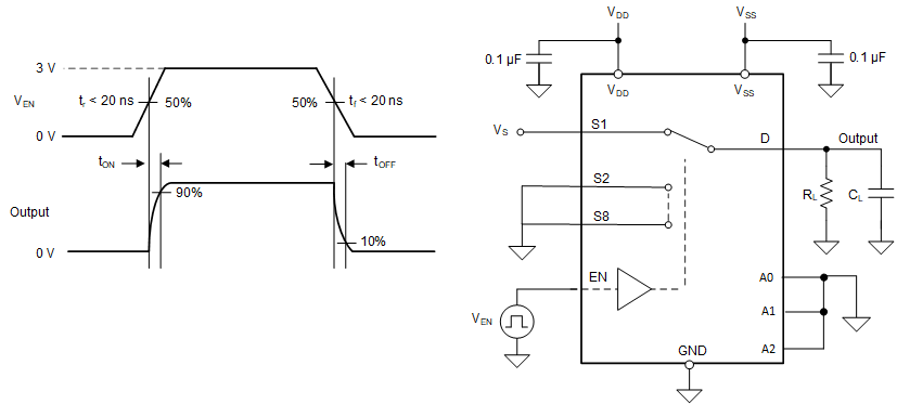
Turn-on time is defined as the time taken by the output of the device to rise to 90% after the enable has risen past the logic threshold. The 90% measurement is utilized to provide the timing of the device. System level timing can then account for the time constant added from the load resistance and load capacitance. Figure 8-7 shows the setup used to measure turn-on time, denoted by the symbol tON(EN).
Turn-off time is defined as the time taken by the output of the device to fall to 10% after the enable has fallen past the logic threshold. The 10% measurement is utilized to provide the timing of the device. System level timing can then account for the time constant added from the load resistance and load capacitance. Figure 8-7 shows the setup used to measure turn-off time, denoted by the symbol tOFF(EN).
 Figure 8-5 Turn-On and
Turn-Off Time Measurement Setup