SCDS403C february 2021 – july 2023 TMUX7308F , TMUX7309F
PRODUCTION DATA
- 1
- 1 Features
- 2 Applications
- 3 Description
- 4 Revision History
- 5 Device Comparison Table
- 6 Pin Configuration and Functions
-
7 Specifications
- 7.1 Absolute Maximum Ratings
- 7.2 ESD Ratings
- 7.3 Thermal Information
- 7.4 Recommended Operating Conditions
- 7.5 Electrical Characteristics (Global)
- 7.6 ±15 V Dual Supply: Electrical Characteristics
- 7.7 ±20 V Dual Supply: Electrical Characteristics
- 7.8 12 V Single Supply: Electrical Characteristics
- 7.9 36 V Single Supply: Electrical Characteristics
- 7.10 Typical Characteristics
-
8 Parameter Measurement Information
- 8.1 On-Resistance
- 8.2 Off-Leakage Current
- 8.3 On-Leakage Current
- 8.4 Input and Output Leakage Current Under Overvoltage Fault
- 8.5 Break-Before-Make Delay
- 8.6 Enable Delay Time
- 8.7 Transition Time
- 8.8 Fault Response Time
- 8.9 Fault Recovery Time
- 8.10 Charge Injection
- 8.11 Off Isolation
- 8.12 Crosstalk
- 8.13 Bandwidth
- 8.14 THD + Noise
- 9 Detailed Description
- 10Application and Implementation
- 11Device and Documentation Support
- 12Mechanical, Packaging, and Orderable Information
Package Options
Mechanical Data (Package|Pins)
Thermal pad, mechanical data (Package|Pins)
Orderable Information
6 Pin Configuration and Functions
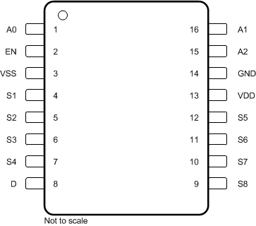
 Figure 6-1 PW Package, 16-Pin TSSOP
(Top View)
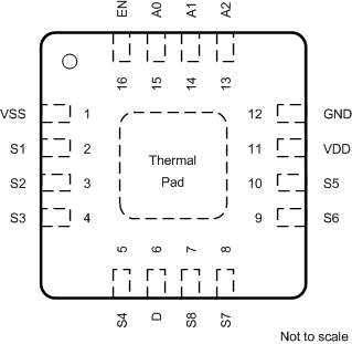
 Figure 6-2 RRP Package, 16-Pin WQFN
(Top View)
Figure 6-2 RRP Package, 16-Pin WQFN
(Top View)Table 6-1 Pin Functions: TMUX7308F
| PIN | TYPE(1) | DESCRIPTION | ||
|---|---|---|---|---|
| NAME | TSSOP | WQFN | ||
| A0 | 1 | 15 | I | Logic control input address 0 (A0), has internal 4 MΩ pull-down resistor. Controls switch state as shown in Section 9.4.3. |
| EN | 2 | 16 | I | Active high logic enable (EN) pin, has internal 4 MΩ pull-down resistor. The device is disabled and all switches become high impedance when the pin is low. When the pin is high, the Ax logic inputs determine individual switch states as shown in Section 9.4.3. |
| VSS | 3 | 1 | P | Negative power supply. This pin is the most negative power-supply potential. In single-supply applications, this pin can be connected to ground. For reliable operation, connect a decoupling capacitor ranging from 0.1 µF to 10 µF between VSS and GND. |
| S1 | 4 | 2 | I/O | Overvoltage protected source pin 1. Can be an input or output. |
| S2 | 5 | 3 | I/O | Overvoltage protected source pin 2. Can be an input or output. |
| S3 | 6 | 4 | I/O | Overvoltage protected source pin 3. Can be an input or output. |
| S4 | 7 | 5 | I/O | Overvoltage protected source pin 4. Can be an input or output. |
| D | 8 | 6 | I/O | Drain pin. Can be an input or output. The drain pin is not overvoltage protected. |
| S8 | 9 | 7 | I/O | Overvoltage protected source pin 8. Can be an input or output. |
| S7 | 10 | 8 | I/O | Overvoltage protected source pin 7. Can be an input or output. |
| S6 | 11 | 9 | I/O | Overvoltage protected source pin 6. Can be an input or output. |
| S5 | 12 | 10 | I/O | Overvoltage protected source pin 5. Can be an input or output. |
| VDD | 13 | 11 | P | Positive power supply. This pin is the most positive power-supply potential. For reliable operation, connect a decoupling capacitor ranging from 0.1 µF to 10 µF between VDD and GND. |
| GND | 14 | 12 | P | Ground (0 V) reference |
| A2 | 15 | 13 | I | Logic control input address 2 (A2), has internal 4 MΩ pull-down resistor. Controls switch state as shown in Section 9.4.3. |
| A1 | 16 | 14 | I | Logic control input address 1 (A1), has internal 4 MΩ pull-down resistor. Controls switch state as shown in Section 9.4.3. |
| Thermal Pad | P | The thermal pad is not connected internally. It is recommended that the pad be tied to GND or VSS for best performance. | ||
(1) I = input, O = output, I/O = input and output, P = power
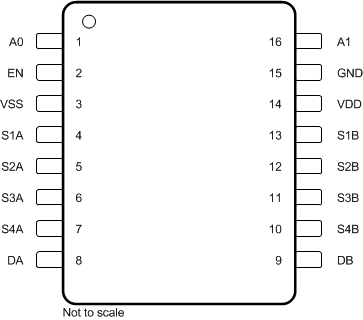
 Figure 6-3 PW Package, 16-Pin TSSOP
(Top View)
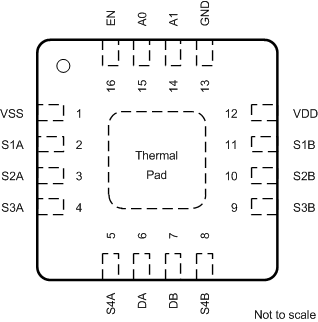
 Figure 6-4 RRP Package, 16-Pin WQFN
(Top View)
Figure 6-4 RRP Package, 16-Pin WQFN
(Top View)Table 6-2 Pin Functions: TMUX7309F
| PIN | TYPE(1) | DESCRIPTION | ||
|---|---|---|---|---|
| NAME | TSSOP | WQFN | ||
| A0 | 1 | 15 | I | Logic control input address 0 (A0), has internal 4 MΩ pull-down resistor. Controls switch state as shown in Section 9.4.3. |
| EN | 2 | 16 | I | Active high logic enable (EN) pin, has internal 4 MΩ pull-down resistor. The device is disabled and all switches become high impedance when the pin is low. When the pin is high, the Ax logic inputs determine individual switch states as shown in Section 9.4.3. |
| VSS | 3 | 1 | P | Negative power supply. This pin is the most negative power-supply potential. In single-supply applications, this pin can be connected to ground. For reliable operation, connect a decoupling capacitor ranging from 0.1 µF to 10 µF between VSS and GND. |
| S1A | 4 | 2 | I/O | Overvoltage protected source pin 1A. Can be an input or output. |
| S2A | 5 | 3 | I/O | Overvoltage protected source pin 2A. Can be an input or output. |
| S3A | 6 | 4 | I/O | Overvoltage protected source pin 3A. Can be an input or output. |
| S4A | 7 | 5 | I/O | Overvoltage protected source pin 4A. Can be an input or output. |
| DA | 8 | 6 | I/O | Drain terminal A. Can be an input or output. The drain pin is not overvoltage protected. |
| DB | 9 | 7 | I/O | Drain terminal B. Can be an input or output. The drain pin is not overvoltage protected. |
| S4B | 10 | 8 | I/O | Overvoltage protected source pin 4B. Can be an input or output. |
| S3B | 11 | 9 | I/O | Overvoltage protected source pin 3B. Can be an input or output. |
| S2B | 12 | 10 | I/O | Overvoltage protected source pin 2B. Can be an input or output. |
| S1B | 13 | 11 | I/O | Overvoltage protected source pin 1B. Can be an input or output. |
| VDD | 14 | 12 | P | Positive power supply. This pin is the most positive power-supply potential. For reliable operation, connect a decoupling capacitor ranging from 0.1 µF to 10 µF between VDD and GND. |
| GND | 15 | 13 | P | Ground (0 V) reference |
| A1 | 16 | 14 | I | Logic control input address 1 (A1), has internal 4 MΩ pull-down resistor. Controls switch state as shown in Section 9.4.3. |
| Thermal Pad | P | The thermal pad is not connected internally. It is recommended that the pad be tied to GND or VSS for best performance. | ||
(1) I = input, O = output, I/O = input and output, P = power