SLOS942 April 2018 TPA3126D2
PRODUCTION DATA.
- 1 Features
- 2 Applications
- 3 Description
- 4 Revision History
- 5 Device Comparison Table
- 6 Pin Configuration and Functions
- 7 Specifications
-
8 Detailed Description
- 8.1 Overview
- 8.2 Functional Block Diagram
- 8.3
Feature Description
- 8.3.1 Gain Setting and Master and Slave
- 8.3.2 Input Impedance
- 8.3.3 Startup and Shutdown Operation
- 8.3.4 PLIMIT Operation
- 8.3.5 GVDD Supply
- 8.3.6 BSPx and BSNx Capacitors
- 8.3.7 Differential Inputs
- 8.3.8 Device Protection System
- 8.3.9 DC Detect Protection
- 8.3.10 Short-Circuit Protection and Automatic Recovery Feature
- 8.3.11 Thermal Protection
- 8.3.12 Device Modulation Scheme
- 8.3.13 Efficiency: LC Filter Required with the Traditional Class-D Modulation Scheme
- 8.3.14 Ferrite Bead Filter Considerations
- 8.3.15 When to Use an Output Filter for EMI Suppression
- 8.3.16 AM Avoidance EMI Reduction
- 8.4 Device Functional Modes
- 9 Application and Implementation
- 10Power Supply Recommendations
- 11Layout
- 12Device and Documentation Support
- 13Mechanical, Packaging, and Orderable Information
Package Options
Mechanical Data (Package|Pins)
- DAD|32
Thermal pad, mechanical data (Package|Pins)
- DAD|32
Orderable Information
7.7 Typical Characteristics
fs = 400 kHz, Hybrid Mode, TPA3126D2EVM Tested With AP2722. (unless otherwise noted)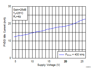 Figure 1. Idle Current vs PVCC
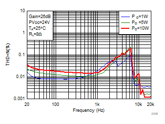 Figure 3. Total Harmonic Distortion + Noise (BTL) vs Frequency
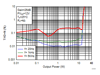 Figure 5. Total Harmonic Distortion + Noise (BTL) vs Output Power
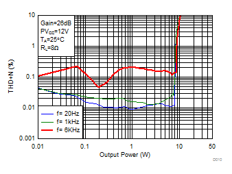 Figure 7. Total Harmonic Distortion + Noise (BTL) vs Output Power
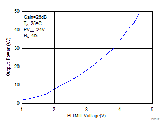 Figure 9. Output Power (BTL) vs PLIMIT Voltage
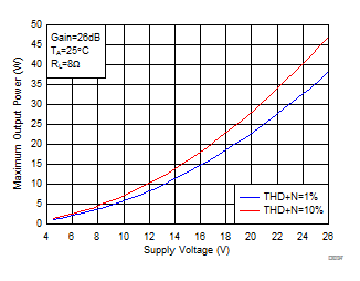 Figure 11. Maximum Output Power (BTL) vs Supply Voltage
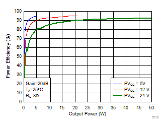 Figure 13. Power Efficiency (BTL) vs Output Power
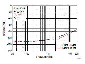 Figure 15. Crosstalk vs Frequency
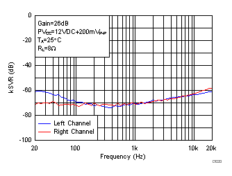 Figure 17. Supply Ripple Rejection Ratio (BTL) vs Frequency
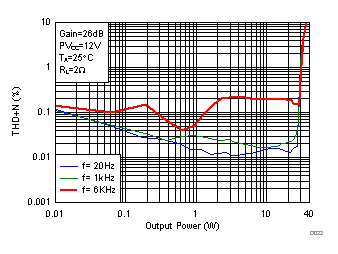 Figure 19. Total Harmonic Distortion + Noise (PBTL) vs Output Power
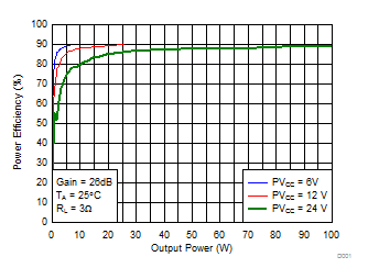 Figure 21. Power Efficiency (PBTL) vs Output Power
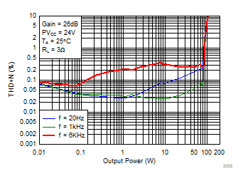 Figure 23. Total Harmonic Distortion + Noise (PBTL) vs Output Power
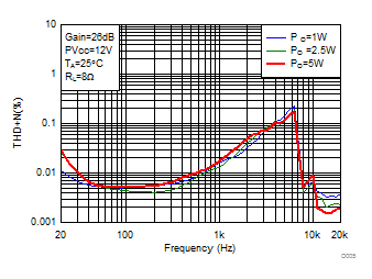 Figure 2. Total Harmonic Distortion + Noise (BTL) vs Frequency
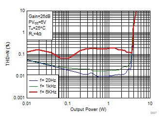 Figure 4. Total Harmonic Distortion + Noise (BTL) vs Output Power
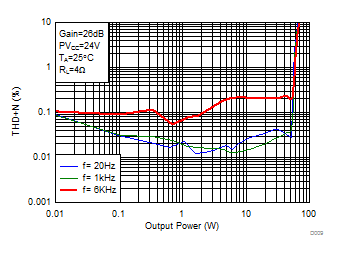 Figure 6. Total Harmonic Distortion + Noise (BTL) vs Output Power
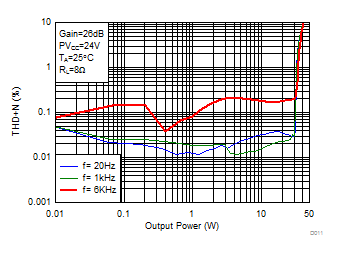 Figure 8. Total Harmonic Distortion + Noise (BTL) vs Output Power
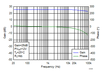 Figure 10. Gain/Phase (BTL) vs Frequency
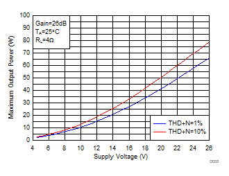 Figure 12. Maximum Output Power (BTL) vs Supply Voltage
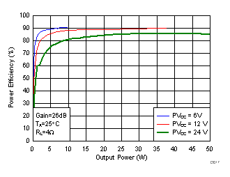 Figure 14. Power Efficiency (BTL) vs Output Power
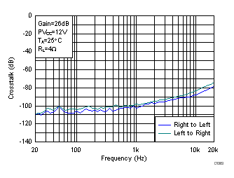 Figure 16. Crosstalk vs Frequency
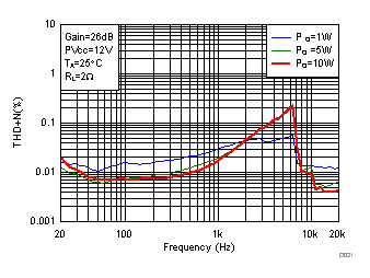 Figure 18. Total Harmonic Distortion + Noise (PBTL) vs Frequency
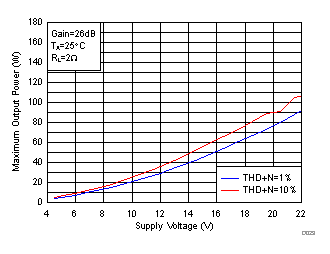 Figure 20. Maximum Output Power (PBTL) vs Supply Voltage
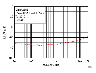 Figure 22. Supply Ripple Rejection Ratio (PBTL) vs Frequency
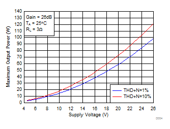 Figure 24. Maximum Output Power (PBTL) vs Supply Voltage