SLOS431B March 2004 – February 2015 TPA6120A2
PRODUCTION DATA.
- 1 Features
- 2 Applications
- 3 Description
- 4 Simplified Schematic
- 5 Revision History
- 6 Pin Configuration and Functions
- 7 Specifications
- 8 Parameter Measurement Information
- 9 Detailed Description
- 10Applications and Implementation
- 11Power Supply Recommendations
- 12Layout
- 13Device and Documentation Support
- 14Mechanical, Packaging, and Orderable Information
Package Options
Refer to the PDF data sheet for device specific package drawings
Mechanical Data (Package|Pins)
- RGY|14
- DWP|20
Thermal pad, mechanical data (Package|Pins)
Orderable Information
10 Applications and Implementation
NOTE
Information in the following applications sections is not part of the TI component specification, and TI does not warrant its accuracy or completeness. TI’s customers are responsible for determining suitability of components for their purposes. Customers should validate and test their design implementation to confirm system functionality.
10.1 Application Information
In many applications, the audio source is digital, and must go through a digital-to-analog converter (DAC) so that traditional analog amplifiers can drive the speakers or headphones.
10.2 Typical Application
10.2.1 High Voltage, High Fidelity DAC + Headphone Amplifier Solution
Figure 13 shows a complete circuit schematic for such a system. The digital audio is fed into a high performance DAC. The PCM1792, a Burr-Brown product from TI, is a 24-bit, stereo DAC.
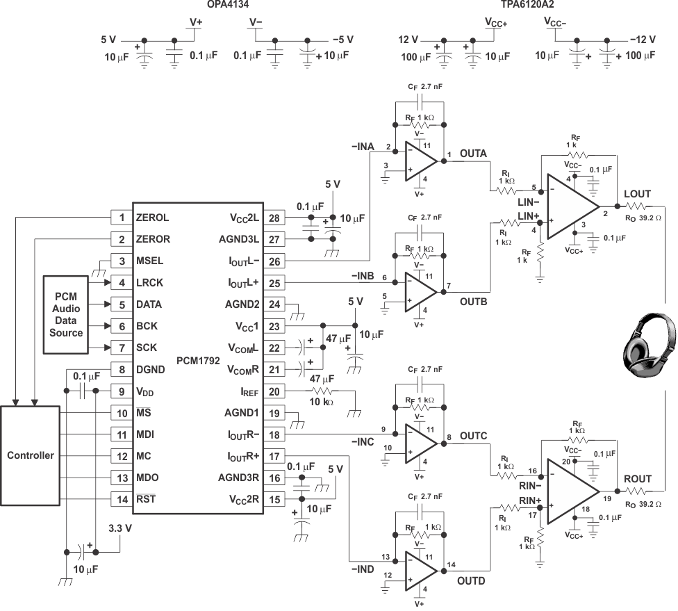 Figure 13. Typical Application Circuit
10.2.1.1 Design Requirements
- ±12V Operation from bipolar power supply
- Differential voltage source
- Be transparent to the user
10.2.1.2 Detailed Design Procedure
The output of the PCM1792 is current, not voltage, so the OPA4134 is used to convert the current input to a voltage output. The OPA4134 (SBOS058), is a low-noise, high-speed, high-performance operational amplifier. CF and RF are used to set the cutoff frequency of the filter. The RC combination in Figure 13 has a cutoff frequency of 59 kHz. All four amplifiers of the OPA4134 are used so the TPA6120A2 can be driven differentially.
The output of the OPA4134 goes into the TPA6120A2. The TPA6120A2 is configured for use with differential inputs, stereo use, and a gain of 2V/V. Note that the 0.1µF capacitors are placed at every supply pin of the TPA6120A2, as well as the 39.2Ω series output resistor.
Each output goes to one channel of a pair of stereo headphones, where the listener enjoys crisp, clean, virtually noise free music with a dynamic range greater than the human ear is capable of detecting.
10.2.1.2.1 Resistor Values
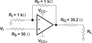 Figure 14. Single-Ended Input With A Noninverting Gain Of 2V/V
In the most basic configuration (see Figure 14), four resistors must be considered, not including the load impedance. The feedback and input resistors, RF and RI, respectively, determine the closed-loop gain of the amplifier. RO is a series output resistor designed to protect the amplifier from any capacitance on the output path, including board and load capacitance. RS is a series input resistor.
The series output resistor should be between 10Ω and 100Ω. The output series resistance eases the work of the output power stage by increasing the load when low impedance headphones are connected, as well as isolating any capacitance on the following traces and headphone cable.
Because the TPA6120A2 is a current-feedback amplifier, take care when choosing the feedback resistor. TI recommends a lower level of 800Ω for the feedback resistance. No capacitors should be used in the feedback path, as they will form a short circuit at high frequencies.
The value of the feedback resistor should be chosen by using Figure 17 as a guideline. The gain can then be set by adjusting the input resistor. The smaller the feedback resistor, the less noise is introduced into the system. However, smaller values move the dominant pole to higher and higher frequencies, making the device more susceptible to oscillations. Higher feedback resistor values add more noise to the system, but pull the dominant pole down to lower frequencies, making the device more stable. Higher impedance loads tend to make the device more unstable. One way to combat this problem is to increase the value of the feedback resistor. It is not recommended that the feedback resistor exceed a value of 10kΩ. The typical value for the feedback resistor for the TPA6120A2 is 1kΩ. In some cases, where a high-impedance load is used along with a relatively large gain and a capacitive load, it may be necessary to increase the value of the feedback resistor from 1kΩ to 2kΩ, thus adding more stability to the system. Another method to deal with oscillations is to increase the size of RO.
CAUTION
Do not place a capacitor in the feedback path. Doing so can cause oscillations.
Capacitance at the outputs can cause oscillations. Capacitance from some sources, such as layout, can be minimized. Other sources, such as those from the load (for example, the inherent capacitance in a pair of headphones), cannot be easily minimized. In this case, adjustments to RO and/or RF may be necessary.
The series output resistor should be kept at a minimum of 10Ω; small enough so that the effect on the load is minimal, but large enough to provide the protection necessary such that the output of the amplifier sees little capacitance. The value can be increased to provide further isolation, up to 100Ω. Care should be taken in selecting the thermal capacity of the output series resistor, as it will create a potential divider with the load and dissipate power.
The series resistor, RS, should be used for two reasons:
- It prevents the positive input pin from being exposed to capacitance from the line and source.
- It prevents the source from seeing the input capacitance of the TPA6120A2.
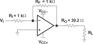 Figure 15. Single-Ended Input With A Noninverting Gain Of –1V/V
Figure 16 shows the TPA6120A2 connected with differential inputs. Differential inputs are useful because they take the greatest advantage of the high CMRR of the device. The two feedback resistor values must be kept the same, as do the input resistor values.
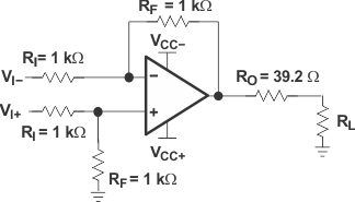 Figure 16. Differential Input With A Noninverting Gain Of 2V/V
Special note regarding mono operation:
- If both amplifiers are powered on, but only one channel is to be used, the unused amplifier MUST have a feedback resistor from the output to the negative input. Additionally, the positive input should be grounded as close to the pin as possible. Terminate the output as close to the output pin as possible with a 25Ω load to ground.
- These measures should be followed to prevent the unused amplifier from oscillating. If it oscillates, and the power pins of both amplifiers are tied together, the performance of the amplifier could be seriously degraded.
10.2.1.2.2 Checking For Oscillations And Instability
Checking the stability of the amplifier setup is recommended. High frequency oscillations in the megahertz region can cause undesirable effects in the audio band.
Sometimes, the oscillations can be quite clear. An unexpectedly large draw from the power supply may be an indication of oscillations. These oscillations can be seen with an oscilloscope. However, if the oscillations are not obvious, or there is a chance that the system is stable but close to the edge, placing a scope probe with 10pF of capacitance can make the oscillations worse, or actually cause them to start.
A network analyzer can be used to determine the inherent stability of a system. An output versus frequency curve generated by a network analyzer can be a good indicator of stability. At high frequencies, the curve shows whether a system is oscillating, close to oscillation, or stable. In Figure 17 the system is stable because the high frequency rolloff is smooth and has no peaking. Increasing RF decreases the frequency at which this rolloff occurs (see the Resistor Values section). Another scenario shows some peaking at high frequency. If the peaking is 2dB, the amplifier is stable as there is still 45 degrees of phase margin. As the peaking increases, the phase margin shrinks, causing the amplifier and the system to approach instability. The same system that normally has a 2dB peak has an increased peak when a capacitor is added to the output, indicating that the system is either on the verge of oscillation or is oscillating; corrective action is required.
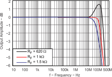
| VCC = ±5V | Gain = 1V/V | RL = 25Ω | ||
| VIN = 200mV |
10.2.1.2.3 Thermal Considerations
There is no one to one relationship between output power and heat dissipation, so the following equations must be used:
Where

Where
Therefore,
| PL = Power delivered to load (per channel) |
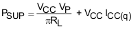
| PSUP = Power drawn from power supply |
| VLRMS = RMS voltage on the load |
| RL = Load resistance |
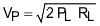
| VP = Peak voltage on the load |
| ICCavg = Average current drawn from the power supply |
| ICC(q) = Quiescent current (per channel) |
| VCC = Power supply voltage (total supply voltage = 30 V if running on a ±15-V power supply |
| η = Efficiency of a SE amplifier |
For stereo operation, the efficiency does not change because both PL and PSUP are doubled, affecting the amount of power dissipated by the package in the form of heat.
A simple formula for calculating the power dissipated, PDISS, is shown in Equation 7:

In stereo operation, PSUP is twice the quantity that is present in mono operation.
The maximum ambient temperature, TA, depends on the heat-sinking ability of the system. RθJA for a 20-pin DWP, whose thermal pad is properly soldered down, is shown in Thermal Information. Also see Figure 18.

10.2.1.3 Application Performance Plots
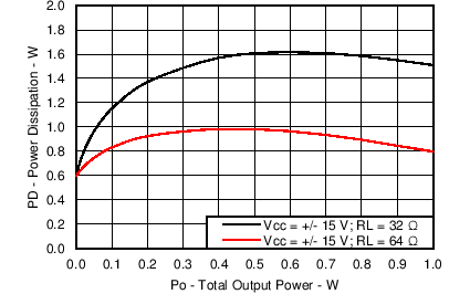 Figure 18. Power Dissipation versus Output Power
10.2.2 High Fidelity Smartphone Application
A new trend in portable applications are termed "Hifi Smartphones". In these systems, a standard portable audio codec continues to be used for telephony, while a separate, higher performance DAC and Headphone Amplifier is used for music playback.
Figure 19 shows a complete circuit schematic for such a system. The digital audio is fed into a high performance DAC. The PCM5242, a Burr-Brown product from TI, is a 32-bit, stereo DAC.
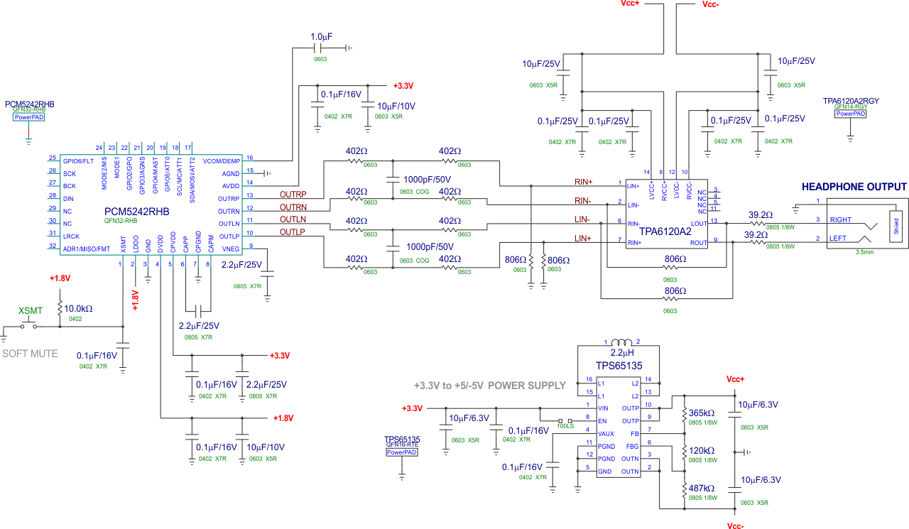 Figure 19. Typical Application Circuit
10.2.2.1 Design Requirements
- ±5V Operation from an over system power supply of 3.3V
- Stereo differential inputs (DAC is differential)
- Be transparent to the user. (DAC SNR and THD+N performance all the way to the headphone)
10.2.2.2 Detailed Design Procedure
For optimal performance, the TPA6120A2 is configured for use with differential inputs, stereo use, and a gain of 1V/V.
The TPA6120A2 requires a bipolar power supply to drive a ground centered output. The application employs a TPS65135 DC-DC converter that generates ±5V from a single 3.3V supply.
The PCM5242 DAC is configured for a 1VRMS output so that clipping is avoided should the 3.3V power supply sag. The PCM5242 offers a ground centered output, so that no DC blocking capacitors are required between it and the TPA6120A2.
Resistor values around the TPA6120A2 of 806Ω and a 39.2Ω were found to offer the optimal conditions of SNR and THD. Starting with 1KΩ resistors for input and feedback, and 10Ω output resistance, the feedback resistance was lowered to increase the amount of current in the feedback network. The output resistance was increased to ease the load on the headphone amplifier when low impedance headphones are connected. Both of these additions contribute to the excellent SNR and THD of the TPA6120A2 in such a low voltage application.
Note that the 0.1-uF X7R capacitors are placed at every supply pin of the TPA6120A2.
Using such a solution makes the TPA6120A2 transparent in the circuit, even into a low impedance 32Ohm load.
The remaining steps are the same as those described in Resistor Values.
10.2.2.3 Application Performance Plots
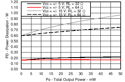 Figure 20. Power Dissipation versus Power Output - 50mW Scale
In this particular application, the TPA6120A2's performance is transparent and the performance of the system is dictated by the PCM5242 DAC.