SLOS431B March 2004 – February 2015 TPA6120A2
PRODUCTION DATA.
- 1 Features
- 2 Applications
- 3 Description
- 4 Simplified Schematic
- 5 Revision History
- 6 Pin Configuration and Functions
- 7 Specifications
- 8 Parameter Measurement Information
- 9 Detailed Description
- 10Applications and Implementation
- 11Power Supply Recommendations
- 12Layout
- 13Device and Documentation Support
- 14Mechanical, Packaging, and Orderable Information
Package Options
Refer to the PDF data sheet for device specific package drawings
Mechanical Data (Package|Pins)
- RGY|14
- DWP|20
Thermal pad, mechanical data (Package|Pins)
Orderable Information
7 Specifications
7.1 Absolute Maximum Ratings
over operating free-air temperature range (unless otherwise noted) (1)| MIN | MAX | UNIT | |
|---|---|---|---|
| Supply voltage, xVCC+ to xVCC- Where x=L or R channel | 9 | 33 | V |
| Input voltage, VI(2) | ± VCC | ||
| Differential input voltage, VID | 6 | V | |
| Minimum load impedance | 8 | Ω | |
| Continuous total power dissipation | See Thermal Information | ||
| Operating free–air temperature range, TA | –40 | 85 | °C |
| Operating junction temperature range, TJ(3) | –40 | 150 | °C |
| Storage Temperature, Tstg | –40 | 125 | °C |
(1) Stresses beyond those listed under “absolute maximum ratings” may cause permanent damage to the device. These are stress ratings only, and functional operation of the device at these or any other conditions beyond those indicated under “recommended operating conditions” is not implied. Exposure to absolute–maximum–rated conditions for extended periods may affect device reliability.
(2) When the TPA6120A2 is powered down, the input source voltage must be kept below 600mV peak.
(3) The TPA6120A2 incorporates an exposed PowerPAD on the underside of the chip. This acts as a heatsink and must be connected to a thermally dissipating plane for proper power dissipation. Failure to do so may result in exceeding the maximum junction temperature that could permanently damage the device. See TI Technical Brief SLMA002 for more information about utilizing the PowerPAD thermally enhanced package.
7.2 ESD Ratings
| VALUE | UNIT | ||||
|---|---|---|---|---|---|
| V(ESD) | Electrostatic Discharge | Human body model (HBM), per ANSI/ESDA/JEDEC JS-001(1) | For Pins: LVCC+, RVCC+, LVCC-, RVCC | ±500 | V |
| Human body model (HBM), per ANSI/ESDA/JEDEC JS-001, all other pins | For all pins except: LVCC+, RVCC+, LVCC-, RVCC | ±2000 | |||
| Charged device model (CDM), per JEDEC specification JESD22-C101 | ±1500 | ||||
(1) Level listed above is the passing level per ANSI, ESDA, and JEDEC JS-001. JEDEC document JEP155 states that 500V HBM allows safe manufacturing with a standard ESD control process.
7.3 Recommended Operating Conditions
| MIN | NOM | MAX | UNIT | ||
|---|---|---|---|---|---|
| Supply voltage, VCC+ and VCC- | Split Supply | ±5 | ±15 | V | |
| Single Supply | 10 | 30 | |||
| Load impedance | VCC = ±5V or ±15V | 16 | Ω | ||
| Operating free–air temperature, TA | –40 | 85 | °C |
7.4 Thermal Information
| THERMAL METRIC(1) | TPA6120A2 | TPA6120A2 | UNIT | |
|---|---|---|---|---|
| DWP [HSOP] | RGY [VQFN] | |||
| 20 PINS | 14 PINS | |||
| RθJA | Junction-to-ambient thermal resistance | 44.5 | 49.4 | °C/W |
| RθJCtop | Junction-to-case (top) thermal resistance | 55.2 | 62.0 | |
| RθJB | Junction-to-board thermal resistance | 36.1 | 25.4 | |
| ψJT | Junction-to-top characterization parameter | 23.1 | 1.6 | |
| ψJB | Junction-to-board characterization parameter | 36.2 | 25.5 | |
| RθJCbot | Junction-to-case (bottom) thermal resistance | 7.6 | 6.2 | |
(1) For more information about traditional and new thermal metrics, see the IC Package Thermal Metrics application report, SPRA953.
7.5 Electrical Characteristics
over operating free-air temperature range (unless otherwise noted)7.6 Operating Characteristics(1)
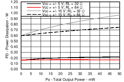
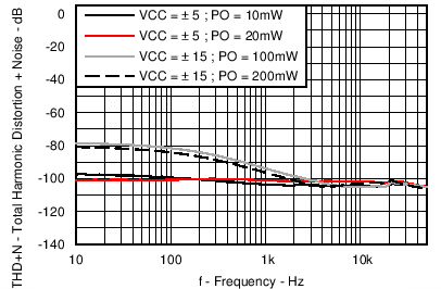
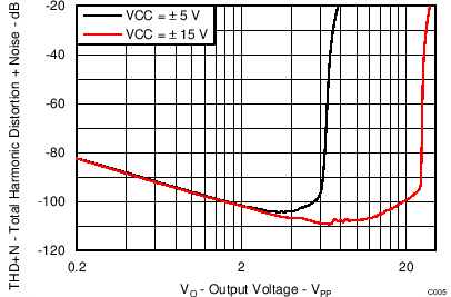
TA = 25°C, RL = 25Ω, Gain = 1V/V (unless otherwise noted)(1) For THD+N, kSVR, and crosstalk, the bandwidth of the measurement instruments was set to 80kHz.
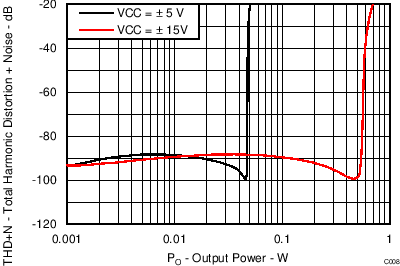
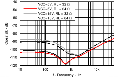
7.7 Typical Characteristics
| RL = 10kΩ | Gain = 3V/V | RF = 2kΩ |
| RI = 1kΩ | BW = 80kHz | |
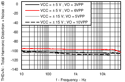
| RL = 32Ω | Gain = 3V/V | RF = 2kΩ |
| RI = 1kΩ | BW = 80kHz | |
| RL = 64Ω | Gain = 3V/V | RF = 2kΩ |
| RI = 1kΩ | BW = 80kHz | f = 1kHz |
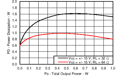
| Mono | VCC = ±15V | |
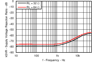
| VCC = ±5V | V(ripple) = 1VPP | Gain = 2V/V |
| BW = 80kHz | ||
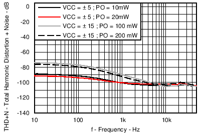
| RL = 64Ω | Gain = 3V/V | RF = 2kΩ |
| RI = 1kΩ | BW = 80kHz | |
| RL = 10kΩ | Gain = 3V/V | RF = 2kΩ |
| RI = 1kΩ | BW = 80kHz | f = 1kHz |
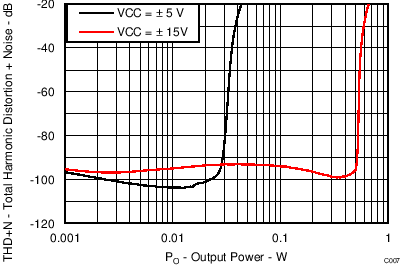
| RL = 32Ω | Gain = 3V/V | RF = 2kΩ |
| RI = 1kΩ | BW = 80kHz | f = 1kHz |
| VCC = ±12V | V(ripple) = 1VPP | Gain = 2V/V |
| BW = 80kHz | ||
| Representative of both positive and negative supplies | ||
| RF = 1kΩ | Gain = 2V/V | BW = 80kHz |