SLOS431B March 2004 – February 2015 TPA6120A2
PRODUCTION DATA.
- 1 Features
- 2 Applications
- 3 Description
- 4 Simplified Schematic
- 5 Revision History
- 6 Pin Configuration and Functions
- 7 Specifications
- 8 Parameter Measurement Information
- 9 Detailed Description
- 10Applications and Implementation
- 11Power Supply Recommendations
- 12Layout
- 13Device and Documentation Support
- 14Mechanical, Packaging, and Orderable Information
Package Options
Refer to the PDF data sheet for device specific package drawings
Mechanical Data (Package|Pins)
- RGY|14
- DWP|20
Thermal pad, mechanical data (Package|Pins)
Orderable Information
12 Layout
12.1 Layout Guidelines
Proper board layout is crucial to getting the maximum performance out of the TPA6120A2.
A ground plane should be used on the board to provide a low inductive ground connection. Having a ground plane underneath traces adds capacitance, so care must be taken when laying out the ground plane on the underside of the board (assuming a 2-layer board). The ground plane is necessary on the bottom for thermal reasons.
Stray capacitance can still make its way onto the sensitive outputs and inputs. Place components as close as possible to the pins and reduce trace lengths. See Figure 21 and Figure 22. Place the feedback resistor and the series output resistor extremely close to the pins. The input resistor should also be placed close to the pin. If the amplifier is to be driven in a noninverting configuration, ground the input close to the device so the current has a short, straight path to the PowerPAD (gnd).
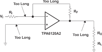 Figure 21. Layout That Can Cause Oscillation
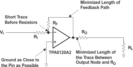 Figure 22. Layout Designed To Reduce Capacitance On Critical Nodes
12.2 Layout Example
This is part of a 4-layer board, where ground, V+, V- are on the bottom and two middle traces, respectively. Key items to note in this layout:
- R4 and R3 are the output resistors in the schematic. They are sized as 0603 surface mount resistors instead of 0402 for their thermal capacity, as they will be dissipating heat, depending on the output power.
- Traces are kept as short as possible to avoid any capacitance or oscillation issues.
- In systems that may be using the DWP package with through hole resistors, it's strongly suggested that the input and output pins and components do not have a ground plane directly beneath them, to avoid stray capacitance.
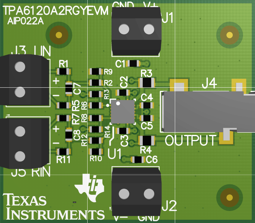 Figure 23. PCB Layout Example
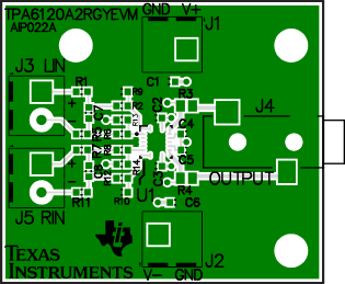 Figure 24. Example PCB Layout, Top Layer and Silkscreen, Top View
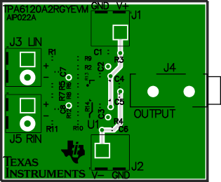 Figure 26. Example PCB Layout, Middle-2 Layer and Silkscreen, Top View
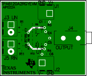 Figure 25. Example PCB Layout, Middle-1 Layer and Silkscreen, Top View
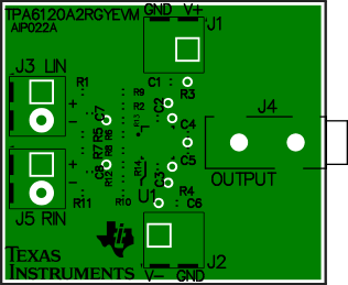 Figure 27. Example PCB Layout, Bottom Layer and Silkscreen, Top View