SLOS431B March   2004  – February 2015 TPA6120A2

PRODUCTION DATA.  

  1. Features
  2. Applications
  3. Description
  4. Simplified Schematic
  5. Revision History
  6. Pin Configuration and Functions
  7. Specifications
    1. 7.1 Absolute Maximum Ratings
    2. 7.2 ESD Ratings
    3. 7.3 Recommended Operating Conditions
    4. 7.4 Thermal Information
    5. 7.5 Electrical Characteristics
    6. 7.6 Operating Characteristics
    7. 7.7 Typical Characteristics
  8. Parameter Measurement Information
  9. Detailed Description
    1. 9.1 Overview
    2. 9.2 Functional Block Diagram
    3. 9.3 Feature Description
      1. 9.3.1 Current-Feedback Amplifier
      2. 9.3.2 Independent Power Supplies
    4. 9.4 Device Functional Modes
  10. 10Applications and Implementation
    1. 10.1 Application Information
    2. 10.2 Typical Application
      1. 10.2.1 High Voltage, High Fidelity DAC + Headphone Amplifier Solution
        1. 10.2.1.1 Design Requirements
        2. 10.2.1.2 Detailed Design Procedure
          1. 10.2.1.2.1 Resistor Values
          2. 10.2.1.2.2 Checking For Oscillations And Instability
          3. 10.2.1.2.3 Thermal Considerations
        3. 10.2.1.3 Application Performance Plots
      2. 10.2.2 High Fidelity Smartphone Application
        1. 10.2.2.1 Design Requirements
        2. 10.2.2.2 Detailed Design Procedure
        3. 10.2.2.3 Application Performance Plots
  11. 11Power Supply Recommendations
    1. 11.1 Independent Power Supplies
    2. 11.2 Power Supply Decoupling
  12. 12Layout
    1. 12.1 Layout Guidelines
    2. 12.2 Layout Example
  13. 13Device and Documentation Support
    1. 13.1 Documentation Support
      1. 13.1.1 Related Documentation
    2. 13.2 Trademarks
    3. 13.3 Electrostatic Discharge Caution
    4. 13.4 Glossary
  14. 14Mechanical, Packaging, and Orderable Information

Package Options

Refer to the PDF data sheet for device specific package drawings

Mechanical Data (Package|Pins)
  • RGY|14
  • DWP|20
Thermal pad, mechanical data (Package|Pins)
Orderable Information

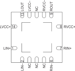
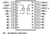
6 Pin Configuration and Functions

DWP Package
20-Pin HSOP
Top View
po_los431.gif
RGY Package
14-Pin VQFN with Thermal PAD
Top View
po_rgy.gif

Pin Functions

PIN I/O DESCRIPTIONS
NAME HSOP NO. VQFN NO.
LVCC- 1 12 I Left channel negative power supply – must be kept at the same potential as RVCC- if both amplifiers are to be used.
LOUT 2 13 O Left channel output
LVCC+ 3 14 I Left channel positive power supply – must be kept at the same potential as RVCC+ if both amplifiers are to be used.
LIN+ 4 1 I Left channel positive input
LIN- 5 2 I Left channel negative input
NC 6,7,8,9,10,11,
12,13,14,15
3, 4, 5, 11 - Not internally connected
RIN- 16 6 I Right channel negative input
RIN+ 17 7 I Right channel positive input
RVCC+ 18 8 I Right channel positive power supply - must be kept at the same potential as LVCC+ if both amplifiers are to be used.
ROUT 19 9 O Right channel output
RVCC- 20 10 I Right channel negative power supply - must be kept at the same potential as LVCC- if both amplifiers are to be used.
Thermal Pad - - - Connect to ground. The thermal pad must be soldered down in all applications to properly secure device on the PCB.