SLASEP6B September   2019  – December 2020 TPA6304-Q1

PRODUCTION DATA  

  1. Features
  2. Applications
  3. Description
  4. Revision History
  5. Pin Configuration and Functions
  6. Specifications
    1. 6.1 Absolute Maximum Ratings
    2. 6.2 ESD Ratings
    3. 6.3 Recommended Operating Conditions
    4. 6.4 Thermal Information
    5. 6.5 Electrical Characteristics
    6. 6.6 Typical Characteristics
      1. 6.6.1 Bridge-Tied Load (BTL), BD
      2. 6.6.2 Parallel Bridge-Tied Load (PBTL)
      3. 6.6.3 Bridge-Tied Load (BTL), 1SPW
      4. 6.6.4 Bridge-Tied Load (BTL), 384 kHz, BD
      5. 6.6.5 Bridge-Tied Load (BTL), 384 kHz, 1SPW
  7. Parameter measurement information
  8. Detailed Description
    1. 7.1 Overview
    2. 7.2 Functional Block Diagram
    3. 7.3 Feature Description
      1. 7.3.1  Single-Ended Analog Inputs
      2. 7.3.2  Gain Control
      3. 7.3.3  Class-D Operation and Spread Spectrum Control
        1. 7.3.3.1 High Frequency Pulse Width Modulator (PWM)
        2. 7.3.3.2 Clock Synchronization
        3. 7.3.3.3 Spread Spectrum Control
      4. 7.3.4  Gate Drive
      5. 7.3.5  Power FETs
      6. 7.3.6  Load Diagnostics
        1. 7.3.6.1 DC Load Diagnostics
          1. 7.3.6.1.1 Automatic DC Load Diagnostics at Device Initialization
          2. 7.3.6.1.2 Automatic DC Load Diagnostics During Hi-Z to MUTE or PLAY Transition
          3. 7.3.6.1.3 Manual Start of DC Load Diagnostics
          4. 7.3.6.1.4 Short-to-Ground
          5. 7.3.6.1.5 Short-to-Power
          6. 7.3.6.1.6 Shorted Load and Open Load
          7. 7.3.6.1.7 Line Output Diagnostics
        2. 7.3.6.2 AC Load Diagnostics
          1. 7.3.6.2.1 Operating Principal
          2. 7.3.6.2.2 Stimulus
          3. 7.3.6.2.3 Load Impedance
          4. 7.3.6.2.4 Tweeter Detection
          5. 7.3.6.2.5 Operation
      7. 7.3.7  Power Supply
        1. 7.3.7.1 Power-Supply Sequence
          1. 7.3.7.1.1 Power-Up Sequence
          2. 7.3.7.1.2 Power-Down Sequence
      8. 7.3.8  Device Initialization and Power-On-Reset (POR)
      9. 7.3.9  Protection and Monitoring
        1. 7.3.9.1 Over Current Protection
        2. 7.3.9.2 DC Detect
        3. 7.3.9.3 Load Current Limit
        4. 7.3.9.4 Clip Detect
        5. 7.3.9.5 Temperature Protection and Monitoring
          1. 7.3.9.5.1 Over Temperature Shutdown (OTSD)
          2. 7.3.9.5.2 Over Temperature Warning (OTW)
          3. 7.3.9.5.3 Thermal Gain Foldback (TGFB)
        6. 7.3.9.6 Power Failures
        7. 7.3.9.7 Load Dump Protection
      10. 7.3.10 Hardware Control Pins
        1. 7.3.10.1 FAULT Pin
        2. 7.3.10.2 STANDBY Pin
        3. 7.3.10.3 GPIO Pins
        4. 7.3.10.4 WARNING
        5. 7.3.10.5 MUTE
    4. 7.4 Device Functional Modes
      1. 7.4.1 Internal Reporting Signals
        1. 7.4.1.1 Fault Signal
        2. 7.4.1.2 Warning Signal
        3. 7.4.1.3 Clip Detect Signal
      2. 7.4.2 Device States and Flags
        1. 7.4.2.1 Audio Channel States
          1. 7.4.2.1.1 PROTECTIVE SHUTDOWN with AUTO RECOVERY State
          2. 7.4.2.1.2 PROTECTIVE SHUTDOWN State
            1. 7.4.2.1.2.1 Clear Fault
        2. 7.4.2.2 Status and Memory Registers
          1. 7.4.2.2.1 Status Registers
          2. 7.4.2.2.2 Memory Registers
      3. 7.4.3 Fault Events
        1. 7.4.3.1 Overview
        2. 7.4.3.2 Power Fault Events
          1. 7.4.3.2.1 DVDD POR
          2. 7.4.3.2.2 VBAT Over Voltage Fault
          3. 7.4.3.2.3 VBAT Under Voltage Fault
          4. 7.4.3.2.4 PVDD Over Voltage Fault
          5. 7.4.3.2.5 PVDD Under Voltage Fault
          6. 7.4.3.2.6 GVDD Fault
        3. 7.4.3.3 Over Temperature Shut Down (OTSD) Event
        4. 7.4.3.4 Over Current Shut Down (OCSD) Event
        5. 7.4.3.5 DC Fault Event
        6. 7.4.3.6 Load Current Fault Event
        7. 7.4.3.7 Invalid Clock Fault Event
      4. 7.4.4 Warning Events
        1. 7.4.4.1 Overview
        2. 7.4.4.2 Over Temperature Warning Event
        3. 7.4.4.3 Thermal Gain Foldback Warning Event
        4. 7.4.4.4 Load Current Warning Event
        5. 7.4.4.5 Clip Warning Event
    5. 7.5 Programming
      1. 7.5.1 I2C Serial Communication Bus
        1. 7.5.1.1 I2C Address Selection
      2. 7.5.2 I2C Bus Protocol
        1. 7.5.2.1 Random Write
        2. 7.5.2.2 Sequential Write
        3. 7.5.2.3 Random Read
        4. 7.5.2.4 Sequential Read
    6. 7.6 Register Maps
      1. 7.6.1 Registers
  9. Application Information Disclaimer
    1. 8.1 Application Information
      1. 8.1.1 AM Radio Avoidance
      2. 8.1.2 Parallel BTL Operation (PBTL)
      3. 8.1.3 Reconstruction Filter Design
      4. 8.1.4 Bootstrap Capacitors
      5. 8.1.5 Line Driver Applications
    2. 8.2 Typical Applications
      1. 8.2.1 BTL Application
        1. 8.2.1.1 Design Requirements
        2. 8.2.1.2 Detailed Hardware Design Procedure
      2. 8.2.2 PBTL Application
        1. 8.2.2.1 Detailed Hardware Design Procedure
  10. Power Supply Recommendations
  11. 10Layout
    1. 10.1 Layout Guidelines
      1. 10.1.1 Electrical Connection of Thermal Pad and Heat Sink
      2. 10.1.2 General Considerations
    2. 10.2 Layout Example
    3. 10.3 Thermal Considerations
  12. 11Device and Documentation Support
    1. 11.1 Documentation Support
      1. 11.1.1 Related Documentation
    2. 11.2 Receiving Notification of Documentation Updates
    3. 11.3 Support Resources
    4. 11.4 Trademarks
    5. 11.5 Electrostatic Discharge Caution
    6. 11.6 Glossary

Package Options

Mechanical Data (Package|Pins)
Thermal pad, mechanical data (Package|Pins)
Orderable Information

Device Initialization and Power-On-Reset (POR)

When the system first powers up, or when the DVDD voltage momentarily drops below the POR threshold, the devices initializes.

  • During device initialization all I2C registers are be set to default values.

  • The FAULT Pin is activated and taken low.

  • The I2C device address is determined from the pull-up resistor on the FAULT pin. See I2C Address Selection for details.

  • Once the device finished initialization, the open drain FAULT pin is released.

Figure 7-4 shows the time from DVDD voltage crossing the POR threshold to release of the FAULT pin is approximately 10 ms.

After the initialization, bit 4 of the Power Fault Memory Register indicates that the device went through a POR cycle. Reading this I2C register clears the fault signaling bit.
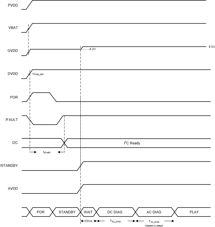
GUID-20201207-CA0I-VXCS-KG6S-MKK1PSLCZPTZ-low.gif Figure 7-4 Typical Initialization Sequence and Timing