SLLSEG9C June   2013  – December  2019 TPD2E2U06

PRODUCTION DATA.  

  1. Features
  2. Applications
  3. Description
    1.     Device Images
      1.      Simplified Schematic
  4. Revision History
  5. Pin Configuration and Functions
    1.     Pin Functions
  6. Specifications
    1. 6.1 Absolute Maximum Ratings
    2. 6.2 ESD Ratings
    3. 6.3 Recommended Operating Conditions
    4. 6.4 Thermal Information
    5. 6.5 Electrical Characteristics
    6. 6.6 Typical Characteristics
  7. Detailed Description
    1. 7.1 Overview
    2. 7.2 Functional Block Diagram
    3. 7.3 Feature Description
      1. 7.3.1 IEC 61000-4-2 Level 4
      2. 7.3.2 IO Capacitance
      3. 7.3.3 DC Breakdown Voltage
      4. 7.3.4 Ultra-Low Leakage Current
      5. 7.3.5 Low ESD Clamping Voltage
      6. 7.3.6 Industrial Temperature Range
      7. 7.3.7 Small Easy-to-Route Package
    4. 7.4 Device Functional Modes
  8. Application and Implementation
    1. 8.1 Application Information
    2. 8.2 Typical Application
      1. 8.2.1 Design Requirements
      2. 8.2.2 Detailed Design Procedure
        1. 8.2.2.1 Signal Range
        2. 8.2.2.2 Operating Frequency
      3. 8.2.3 Application Curves
  9. Power Supply Recommendations
  10. 10Layout
    1. 10.1 Layout Guidelines
    2. 10.2 Layout Example
  11. 11Device and Documentation Support
    1. 11.1 Trademarks
    2. 11.2 Receiving Notification of Documentation Updates
    3. 11.3 Support Resources
    4. 11.4 Glossary
  12. 12Mechanical, Packaging, and Orderable Information

Package Options

Mechanical Data (Package|Pins)
Thermal pad, mechanical data (Package|Pins)
Orderable Information

Pin Configuration and Functions

DRL Package
5-Pin SOT
Top View
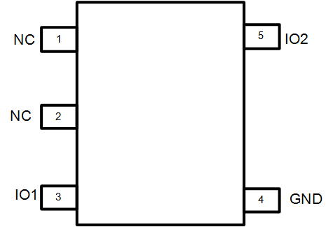
TPD2E2U06 po_sllseg9.gif
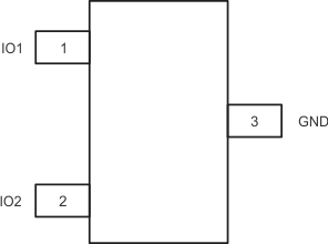
DCK Package
3-Pin SC70
Top View
TPD2E2U06 po_sllsej9.gif

Pin Functions

PIN I/O DESCRIPTION
NAME DRL DCK
IO1 3 1 I/O The IO1 and IO2 pins are an ESD protected channel. Connect these pins to the data line as close to the connector as possible.
IO2 5 2 I/O
NC 1, 2 - This pin is not connected and is left floating, grounded, or connected to VCC.
GND 4 3 G The GND (ground) pin is connected to ground.