SLIS125B December 2006 – December 2014 TPIC74100-Q1
PRODUCTION DATA.
- 1 Features
- 2 Applications
- 3 Description
- 4 Revision History
- 5 Pin Configuration and Functions
- 6 Specifications
-
7 Detailed Description
- 7.1 Overview
- 7.2 Functional Block Diagram
- 7.3
Feature Description
- 7.3.1 Switch-Mode Input/Output Pins (L1, L2)
- 7.3.2 Supply Pin (Vdriver)
- 7.3.3 Internal Supply Decoupling Pin (Vlogic)
- 7.3.4 Input Voltage Monitoring Pin (AIN)
- 7.3.5 Input Undervoltage Alarm Pin (AOUT)
- 7.3.6 Reset Delay Timer Pin (REST)
- 7.3.7 Reset Pin (RESET)
- 7.3.8 Main Regulator Output Pin (VOUT)
- 7.3.9 Low-Power-Mode Pin (CLP)
- 7.3.10 Switch-Output Pin (5Vg)
- 7.3.11 5Vg-Enable Pin (5Vg_ENABLE)
- 7.3.12 Slew-Rate Control Pins (SCR0, SCR1)
- 7.3.13 Modulator Frequency Setting (Pin Rmod)
- 7.3.14 Ground Pin (PGND)
- 7.3.15 Enable Pin (ENABLE)
- 7.3.16 Bootstrap Pins (Cboot1 and Cboot2)
- 7.4 Device Functional Modes
- 8 Applications and Implementation
- 9 Power Supply Recommendations
- 10Layout
- 11Device and Documentation Support
- 12Mechanical, Packaging, and Orderable Information
Package Options
Mechanical Data (Package|Pins)
- PWP|20
Thermal pad, mechanical data (Package|Pins)
- PWP|20
Orderable Information
7 Detailed Description
7.1 Overview
The TPIC74100 is a buck/boost switch-mode regulator that operates in a power-supply concept to ensure a stable output voltage with input voltage excursions and specified load range.
The device provides an alarm indicator and reset output to interface with systems that require supervisory function.
The switching regulator offers a clock modulator and a current-mode slew-rate control for the internal switching transistor (Q1) to minimize EMI.
An internal low-rDS(on) switch has a current-limit feature to prevent inadvertent reset when turning on the 5Vg output.
7.2 Functional Block Diagram
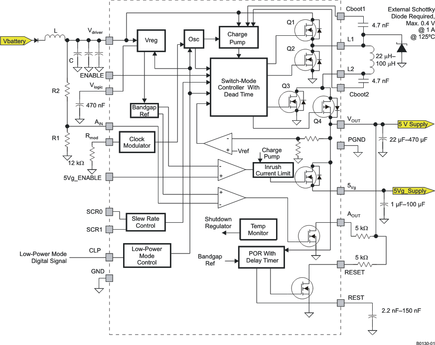
7.3 Feature Description
7.3.1 Switch-Mode Input/Output Pins (L1, L2)
The external inductor for the switch-mode regulator is connected between pins L1 and L2. This inductor is placed close to the pins to minimize parasitic effects. For stability, use an inductor with 20 μH to 100 μH.
7.3.2 Supply Pin (Vdriver)
The input voltage of the device is connected to the Vdriver pin. This input line requires a filter capacitor to minimize noise. A low-ESR aluminum or tantalum input capacitor is recommended. The relevant parameters for the input capacitor are the voltage rating and RMS current rating. The voltage rating should be approximately 1.5 times the maximum applied voltage for an aluminum capacitor and 2 times for a tantalum capacitor. In buck mode, the RMS current is  , where D is the duty cycle and its maximum RMS current value is reached when D = 50% with IRMS = IOUT/2. In boost mode, the RMS current is 0.3 × ΔI, where ΔI is the peak-to-peak ripple current in the inductor. To achieve this, ESR ceramic capacitors are used in parallel with the aluminum or tantalum capacitors.
7.3.3 Internal Supply Decoupling Pin (Vlogic)
The Vlogic pin is used to decouple the internal power-supply noise by use of a 470-nF capacitor. This pin can also be used as an output supply for the logic-level inputs for this device (SCR0, SCR1, ENABLE, CLP, and 5Vg_ENABLE).
7.3.4 Input Voltage Monitoring Pin (AIN)
The AIN pin is used to program the threshold voltage for monitoring and detecting undervoltage conditions on the input supply. A maximum of 40 V may be applied to this pin and the voltage at this pin may exceed the V(driver) input voltage without effecting the device operation. The resistor divider network is programmed to set the undervoltage detection threshold on this pin (see the application schematic). The input has a typical hysteresis of 200 mV with a typical upper limit threshold of 2.5 V and a typical lower limit threshold of 2.3 V. When V(AIN) falls below 2.3 V, V(AOUT) is asserted low; when V(AIN) exceeds 2.5 V, V(AOUT) is in the high-impedance state.
The following equations to set the upper and lower thresholds of V(AIN) are:
7.3.5 Input Undervoltage Alarm Pin (AOUT)
The AOUT pin is an open-drain output that asserts low when the input voltage falls below the set threshold on the AIN input.
7.3.6 Reset Delay Timer Pin (REST)
The REST pin sets the desired delay time to assert the RESET pin low after the 5-V supply has exceeded 4.65 V (typical). The delay can be programmed in the range of 2.2 ms to 150 ms using capacitors in the range of 2.2 nF to 150 nF. The delay time is calculated using Equation 2:
7.3.7 Reset Pin (RESET)
The RESET pin is an open-drain output. The power-on reset output is asserted low until the output voltage exceeds the 4.65-V threshold and the reset delay timer has expired. Additionally, whenever the ENABLE pin is low, RESET is immediately asserted low regardless of the output voltage.
7.3.8 Main Regulator Output Pin (VOUT)
The VOUT pin is the output of the switch-mode regulated supply. This pin requires a filter capacitor with low-ESR characteristics to minimize output ripple voltage. For stability, a capacitor with 22 μF to 470 μF should be used. The total capacitance at pin VOUT and pin 5Vg must be less than or equal to 470 μF.
7.3.9 Low-Power-Mode Pin (CLP)
The CLP pin controls the low-power mode of the device. An external low digital signal switches the device to low-power mode or normal mode when the input is high.
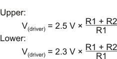
7.3.10 Switch-Output Pin (5Vg)
The 5Vg pin switches the 5-V regulated output. The output voltage of the regulator can be enabled or disabled using this low-rDS(on) internal switch. This switch has a current-limiting function to prevent generation of a reset signal at turn-on caused by the capacitive load on the output or overload condition. When the switch is enabled, the regulated output may deviate and drop momentarily to a tolerance of 7%, until the 5Vg capacitor is fully charged. This deviation depends on the characteristics of the capacitors on VOUT and 5Vg.
7.3.11 5Vg-Enable Pin (5Vg_ENABLE)
The 5Vg_ENABLE is a logic-level input for enabling the switch output on 5Vg.
For the functional pin, 5Vg_ENABLE results in Table 1:
Table 1. 5V-G Enable Pin
| 5Vg_ENABLE | FUNCTION |
|---|---|
| 0 | 5Vg is off |
| Open (internal pulldown = 500 kΩ) | 5Vg is off |
| 1 | 5Vg is on |
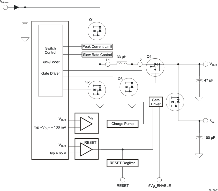 Figure 18. Current-Limit Switched Output 5Vg
7.3.12 Slew-Rate Control Pins (SCR0, SCR1)
The slew rate of the switching transistor Q1 is set using the SCR0 and SCR1 pins.
Table 2 shows the values of the slew rate (SR).
Table 2. Values of the Slew Rate (SR)
| SCR1 | SCR0 | SRQ1 |
|---|---|---|
| 0 | 0 | Slow |
| 0 | 1 | Medium-slow |
| 1 | 0 | Medium-fast |
| 1 | 1 | Fast |
See the converter efficiency plots in the Typical Characteristics section to determine power dissipation.
7.3.13 Modulator Frequency Setting (Pin Rmod)
The Rmod pin adjusts the clock modulator frequency. A resistor of Rmod = 12 kΩ generates a modulation frequency of 28 kHz. The modulator function may be disabled by connecting Rmod to GND and the device operates with the nominal frequency. The modulator function cannot be activated during IC operation, only at IC start-up.
7.3.14 Ground Pin (PGND)
The PGND pin is the power ground for the device.
7.3.15 Enable Pin (ENABLE)
The ENABLE pin allows the enabling and disabling of the switch mode regulator. A maximum of 40 V may be applied to this pin to enable the device and increasing it above the V(driver) input voltage does not affect the device operation.
The functionality of the ENABLE pin is described in Table 3.
Table 3. Enable Pin (ENABLE)
| ENABLE | FUNCTION |
|---|---|
| 0 | Vreg is off. |
| Open | Undefined |
| 1 | Vreg is on. |
7.3.16 Bootstrap Pins (Cboot1 and Cboot2)
An external bootstrap capacitor is required for driving the internal high-side MOSFET switch. A 4.7-nF ceramic capacitor is typically required.
7.4 Device Functional Modes
7.4.1 Clock Modulator
To minimize EMI issues associated with the switch-mode regulator, the device offers an integrated clock modulator. The function of the clock modulator is to modulate the switching frequency and to distribute the energy over the wave band.
The average switching frequency is 440 kHz (typical) and varies between 330 kHz and 550 kHz at a rate set by the Rmod resistor. A typical value of 12 kΩ on the Rmod pin relates to a 28-kHz modulation frequency. The clock modulator function can only be activated during IC start-up, not during IC operation.
The equation for the modulation frequency is as follows:
7.4.2 Buck/Boost Transitioning
The operation mode switches automatically between buck and boost modes depending on the input voltage of V(driver) and output load conditions. During start up, when V(driver) is less than 5.8 V (typical), the device starts in boost mode and continues to run in boost mode until V(driver) exceeds 5.8 V; at which time, the device switches over to buck mode. In buck mode, the device continues to run in buck mode until it is required to switch back to boost to hold regulation. This crossover window to switch to boost mode is when V(driver) is between 5.8 V and 5 V and depends on the loading conditions. When Vdriver drops below 5.8 V but the device is holding regulation (~2%), the device remains in buck mode. However, when V(driver) is within the 5.8-V to 5-V window and VOUT drops to 4.9 V, the device crosses over to boost mode to hold regulation. In boost mode, the device remains in boost mode until V(driver) exceeds 5.8 V; at which time, the device enters the buck mode. When the device is operating in boost mode and V(driver) is in the crossover window of 5.8 V to 5 V, the output regulation may contain a higher than normal ripple and only maintain a 3% tolerance. This ripple and tolerance depends on the loading and improves with a higher loading condition. When the device is operated with low-power mode active (CLP = low) and high output currents (>50 mA), the buck/boost transitioning can cause a reset signal at the RESET pin.
7.4.3 Buck SMPS
In buck mode, the duty cycle of transistor Q1 sets the voltage VOUT. The duty cycle of transistor Q1 varies 10% to 99% depending on the input voltage, V(driver). If the peak inductor current (measured by Q1) exceeds 450 mA (typical), Q2 is turned on for this cycle (synchronized rectification). Otherwise, the current recirculates through Q2 as a free-wheeling diode. The detection for synchronous or asynchronous mode is done cycle-by-cycle.
To avoid a cross-conduction current between Q1 and Q2, an inherent delay is incorporated when switching Q1 off and Q2 on and vice versa.
In buck mode, transistor Q3 is not required and is switched off. Transistor Q4 is switched on to reduce power dissipation.
The switch timings for transistors Q3 and Q4 are not considered. In buck mode, the logical control of the transistors does not change.
 Figure 19. Buck/Boost Switch Mode Configuration
7.4.4 Boost SMPS
In boost mode, the duty cycle of transistor Q3 controls the output voltage VOUT. The duty cycle is internally adjusted 5% to 85% depending on the internally sensed voltage of the output. Synchronized rectification occurs when V(driver) is below 5 V.
To avoid a discharging of the buffer capacitor, a simultaneous switching on of Q3 and Q4 is not allowed. An inherent delay is incorporated between Q3 switching off and Q4 switching on and vice versa.
In boost mode, transistor Q2 is not required and remains off. Transistor Q1 is switched on for the duration of the boost-mode operation (serves as a supply line).
The switch timings of transistors Q1 and Q2 are not considered. In boost mode, the logical control of the transistors does not change.
7.4.5 Extension of the Input Voltage Range on V(driver)
To ensure a stable 5-V output voltage with the output load in the specified range, the V(driver) supply must be greater than or equal to 5 V for greater than 1 ms (typical). After a period of 1 ms (typical), the logic may be supplied by the VOUT regulator and the V(driver) supply may be capable of operating down to 1.5 V.
The switch-mode regulator does not start at V(driver) less than 5 V.
7.4.6 Low-Power Mode
To reduce quiescent current and to provide efficient operation, the regulator enters a pulsed mode.
The device enters this mode by a logic-level low on this pin.
Automatic low-power mode is not available. The low-power-mode function is not available in boost mode. The device leaves low-power mode during boost mode regardless of the logic level on the CLP pin.
7.4.7 Temperature and Short-Circuit Protection
To prevent thermal destruction, the device offers overtemperature protection to disable the IC. Also, short-circuit protection is included for added protection on VOUT and 5Vg.
7.4.8 Switch-Output Pin (5Vg) Current Limitation
A charge pump drives the internal FET, which switches the primary output voltage VOUT to the 5Vg pin. Protection is implemented to prevent the output voltage from dropping below its specified value, while enabling the secondary output voltage. An explanation of the block diagram (see Functional Block Diagram) is given by the following example:
- Device is enabled, output voltage VOUT is up and stable.
- 5Vg is enabled (pin 5Vg_ENABLE set to high) with load resistance connected to the 5Vg pin.
- If output voltage VOUT drops below typical ( VOUT – 100 mV), the charge pump of the 5Vg FET is switched off, and the FET remains on for a while as the gate voltage drops slowly.
- If VOUT drops below the RESET threshold of 4.65 V (typical), the FET of the secondary output voltage 5Vg is switched off (gate drawn to ground level).
- A deglitch time ensures that a device reset does not occur if VOUT drops to the reset level during the 5Vg turn-on phase.
- If VOUT rises above typical (VOUT – 100 mV), the charge pump of the 5Vg FET is switched on and drives the gate of the 5Vg FET on.
7.4.9 Soft Start
On power up, the device offers a soft-start feature which ramps the output of the regulator at a slew of 10 V/ms. When a reset occurs, the soft start is reenabled. Additionally, if the output capacitor is greater than 220 μF (typical), the slew rate decreases to a value set by the internal current limit. In boost mode, the soft-start feature is not active.