SLIS125B December 2006 – December 2014 TPIC74100-Q1
PRODUCTION DATA.
- 1 Features
- 2 Applications
- 3 Description
- 4 Revision History
- 5 Pin Configuration and Functions
- 6 Specifications
-
7 Detailed Description
- 7.1 Overview
- 7.2 Functional Block Diagram
- 7.3
Feature Description
- 7.3.1 Switch-Mode Input/Output Pins (L1, L2)
- 7.3.2 Supply Pin (Vdriver)
- 7.3.3 Internal Supply Decoupling Pin (Vlogic)
- 7.3.4 Input Voltage Monitoring Pin (AIN)
- 7.3.5 Input Undervoltage Alarm Pin (AOUT)
- 7.3.6 Reset Delay Timer Pin (REST)
- 7.3.7 Reset Pin (RESET)
- 7.3.8 Main Regulator Output Pin (VOUT)
- 7.3.9 Low-Power-Mode Pin (CLP)
- 7.3.10 Switch-Output Pin (5Vg)
- 7.3.11 5Vg-Enable Pin (5Vg_ENABLE)
- 7.3.12 Slew-Rate Control Pins (SCR0, SCR1)
- 7.3.13 Modulator Frequency Setting (Pin Rmod)
- 7.3.14 Ground Pin (PGND)
- 7.3.15 Enable Pin (ENABLE)
- 7.3.16 Bootstrap Pins (Cboot1 and Cboot2)
- 7.4 Device Functional Modes
- 8 Applications and Implementation
- 9 Power Supply Recommendations
- 10Layout
- 11Device and Documentation Support
- 12Mechanical, Packaging, and Orderable Information
Package Options
Mechanical Data (Package|Pins)
- PWP|20
Thermal pad, mechanical data (Package|Pins)
- PWP|20
Orderable Information
10 Layout
10.1 Layout Guidelines
10.1.1 Switch-Mode Power Supply
The following guidelines are recommended for PCB layout of the TPIC74100 device.
10.1.1.1 Inductor
Use a low-EMI inductor with a ferrite-type closed core. Other types of inductors may be used; however, they must have low-EMI characteristics and be located away from the low-power traces and components in the circuit.
10.1.1.2 Filter Capacitors
Input ceramic filter capacitors should be located in the close proximity of the Vdriver pin. Surface-mount capacitors are recommended to minimize lead length and reduce noise coupling.
10.1.1.3 Traces and Ground Plane
All power (high-current) traces should be thick and as short as possible. The inductor and output capacitors should be as close to each other as possible. This reduces EMI radiated by the power traces due to high switching currents.
In a two-sided PCB, it is recommended to have ground planes on both sides of the PCB to help reduce noise and ground-loop errors. The ground connection for the input and output capacitors and IC ground should be connected to this ground plane.
In a multilayer PCB, the ground plane is used to separate the power plane (where high switching currents and components are placed) from the signal plane (where the feedback trace and components are) for improved performance.
Also, arrange the components such that the switching-current loops curl in the same direction. Place the high-current components such that during conduction, the current path is in the same direction. This prevents magnetic field reversal caused by the traces between the two half-cycles, helping to reduce radiated EMI.
10.1.2 Package and PCB Land Configuration for a Multilayer PCB
To maximize the efficiency of this package for application on a single-layer or multilayer PCB, certain guidelines must be followed when laying out this device on the PCB.
The following information is to be used as a guideline only.
For further information see the PowerPAD Thermally Enhanced Package technical brief (SLMA002).
The following are guidelines for mounting the PowerPAD™ IC on a multilayer PCB with a ground plane.
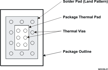 Figure 22. Package and PCB Land Configuration for a Multilayer PCB
10.1.3 Multilayer (Side View)
In a multilayer board application, the thermal vias are the primary method of heat transfer from the package thermal pad to the internal ground plane.
The efficiency of this method depends on several factors (die area, number of thermal vias, thickness of copper, etc.). See the PowerPAD Thermally Enhanced Package technical brief (SLMA002).
Layout recommendation is to use as much copper area for the power-management section of a single-layer board as possible. In a single-layer board application, the thermal pad is attached to a heat spreader (copper areas) by using a low-thermal-impedance attachment method (solder paste or thermal-conductive epoxy). In both of these cases, it is advisable to use as much copper and as many traces as possible to dissipate the heat.
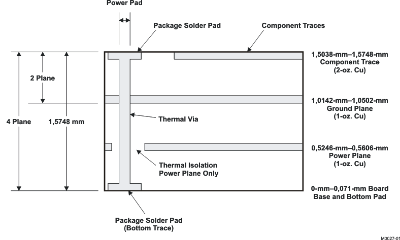 Figure 23. Multilayer Board (Side View)
10.1.4 Single-Layer
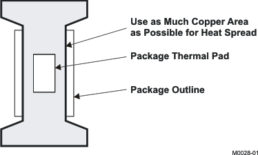 Figure 24. Land Configuration for Single-Layer PCB
| When this attachment method is not implemented correctly, this product may operate inefficiently. Power dissipation capability may be adversely affected when the device is incorrectly mounted onto the circuit board. |
10.2 Layout Example
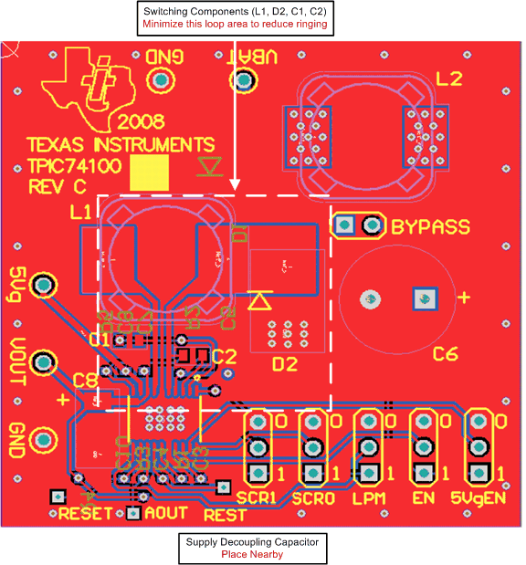 Figure 25. Top Layer
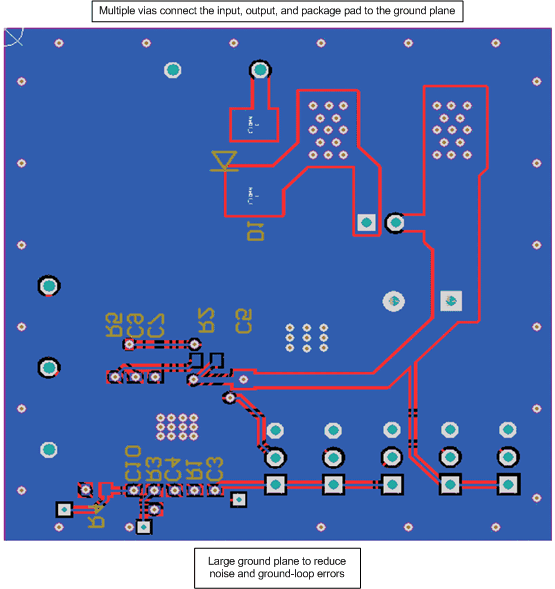 Figure 26. Bottom Layers