SLIS125B December 2006 – December 2014 TPIC74100-Q1
PRODUCTION DATA.
- 1 Features
- 2 Applications
- 3 Description
- 4 Revision History
- 5 Pin Configuration and Functions
- 6 Specifications
-
7 Detailed Description
- 7.1 Overview
- 7.2 Functional Block Diagram
- 7.3
Feature Description
- 7.3.1 Switch-Mode Input/Output Pins (L1, L2)
- 7.3.2 Supply Pin (Vdriver)
- 7.3.3 Internal Supply Decoupling Pin (Vlogic)
- 7.3.4 Input Voltage Monitoring Pin (AIN)
- 7.3.5 Input Undervoltage Alarm Pin (AOUT)
- 7.3.6 Reset Delay Timer Pin (REST)
- 7.3.7 Reset Pin (RESET)
- 7.3.8 Main Regulator Output Pin (VOUT)
- 7.3.9 Low-Power-Mode Pin (CLP)
- 7.3.10 Switch-Output Pin (5Vg)
- 7.3.11 5Vg-Enable Pin (5Vg_ENABLE)
- 7.3.12 Slew-Rate Control Pins (SCR0, SCR1)
- 7.3.13 Modulator Frequency Setting (Pin Rmod)
- 7.3.14 Ground Pin (PGND)
- 7.3.15 Enable Pin (ENABLE)
- 7.3.16 Bootstrap Pins (Cboot1 and Cboot2)
- 7.4 Device Functional Modes
- 8 Applications and Implementation
- 9 Power Supply Recommendations
- 10Layout
- 11Device and Documentation Support
- 12Mechanical, Packaging, and Orderable Information
Package Options
Mechanical Data (Package|Pins)
- PWP|20
Thermal pad, mechanical data (Package|Pins)
- PWP|20
Orderable Information
5 Pin Configuration and Functions
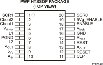
Pin Functions
| PIN | I/O | DESCRIPTION | |
|---|---|---|---|
| NAME | NO. | ||
| SCR1 | 1 | I | Programmable slew-rate control |
| Cboot2 | 2 | I | External bootstrap capacitor |
| Cboot1 | 3 | I | External bootstrap capacitor |
| Vdriver | 4 | I | Input voltage source |
| L1 | 5 | I | Inductor input (an external Schottky diode(1) to GND must be connected to L1) |
| PGND | 6 | I | Power ground |
| L2 | 7 | I | Inductor output |
| VOUT | 8 | O | 5-V regulated output |
| 5Vg | 9 | O | Switched 5-V supply |
| AIN | 10 | I | Programmable alarm setting |
| CLP | 11 | I/O | Low-power operation mode (digital input) |
| RESET | 12 | O | Reset function (open drain) |
| AOUT | 13 | O | Alarm output (open drain) |
| REST | 14 | O | Programmable reset timer delay |
| Rmod | 15 | I | Main switching frequency modulation setting to minimize EMI |
| GND | 16 | I | Ground |
| Vlogic | 17 | O | Supply decoupling output (may be used as a 5-V supply for logic-level inputs) |
| ENABLE | 18 | I | Switch-mode regulator enable/disable |
| 5Vg_ENABLE | 19 | I | Switched 5-V voltage regulator output enable/disable |
| SCR0 | 20 | I | Programmable slew-rate control |
| Exposed thermal pad of the package should be connected to GND or left floating. | |||
(1) Maximum 0.4 V at 1 A and 125°C