SLVSDE7D November   2016  – December 2023 TPS22976

PRODUCTION DATA  

  1.   1
  2. Features
  3. Applications
  4. Description
  5. Device Comparison Table
  6. Pin Configuration and Functions
    1.     Pin Functions
  7. Specifications
    1. 6.1  Absolute Maximum Ratings
    2. 6.2  ESD Ratings
    3. 6.3  Recommended Operating Conditions
    4. 6.4  Thermal Information
    5. 6.5  Electrical Characteristics (VBIAS = 5V)
    6. 6.6  Electrical Characteristics (VBIAS = 2.5V)
    7. 6.7  Switching Characteristics (TPS22976)
    8. 6.8  Switching Characteristics (TPS22976A)
    9. 6.9  Switching Characteristics (TPS22976N)
    10. 6.10 Typical DC Characteristics
    11. 6.11 Typical AC Characteristics
  8. Parameter Measurement Information
  9. Detailed Description
    1. 8.1 Overview
    2. 8.2 Functional Block Diagram
    3. 8.3 Feature Description
      1. 8.3.1 ON and OFF Control
      2. 8.3.2 Input Capacitor (Optional)
      3. 8.3.3 Output Capacitor (Optional)
      4. 8.3.4 Quick Output Discharge (QOD) (Not Present in TPS22976N)
      5. 8.3.5 Thermal Shutdown
    4. 8.4 Device Functional Modes
  10. Application and Implementation
    1. 9.1 Application Information
      1. 9.1.1 Parallel Configuration
      2. 9.1.2 Standby Power Reduction
      3. 9.1.3 Power Supply Sequencing without GPIO Input
      4. 9.1.4 Reverse Current Blocking
    2. 9.2 Typical Application
      1. 9.2.1 Design Requirements
      2. 9.2.2 Detailed Design Procedure
        1. 9.2.2.1 Inrush Current
        2. 9.2.2.2 Adjustable Rise Time
      3. 9.2.3 Application Curves
    3. 9.3 Power Supply Recommendations
    4. 9.4 Layout
      1. 9.4.1 Layout Guidelines
      2. 9.4.2 Layout Example
      3. 9.4.3 Power Dissipation
  11. 10Device and Documentation Support
    1. 10.1 Device Support
      1. 10.1.1 Developmental Support
    2. 10.2 Documentation Support
      1. 10.2.1 Related Documentation
    3. 10.3 Receiving Notification of Documentation Updates
    4. 10.4 Support Resources
    5. 10.5 Trademarks
    6. 10.6 Electrostatic Discharge Caution
    7. 10.7 Glossary
  12. 11Revision History
  13. 12Mechanical, Packaging, and Orderable Information

Package Options

Refer to the PDF data sheet for device specific package drawings

Mechanical Data (Package|Pins)
  • DPU|14
Thermal pad, mechanical data (Package|Pins)
Orderable Information

Typical DC Characteristics

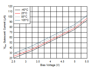
GUID-85C66F5D-6635-493F-B64F-05CE09F1613B-low.gif
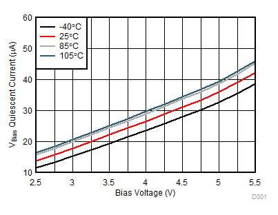
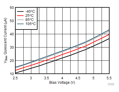
VIN1 = VIN2 = VBIASVON1 = VON2 = 5 VVOUT = Open
Figure 6-1 VBIAS Quiescent Current vs Bias Voltage Both Channels (TPS22976, TPS22976N)
GUID-20200920-CA0I-SZJK-3PR5-TGSPZDVSVCNG-low.gif
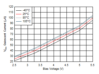
VIN1 = VIN2 = VBIASVON1 = VON2 = 5 VVOUT = Open
Figure 6-3 VBIAS Quiescent Current vs Bias Voltage Both Channels (TPS22976A)
GUID-2C997FDE-C7AF-48BC-A187-2783E16C8B4F-low.gif
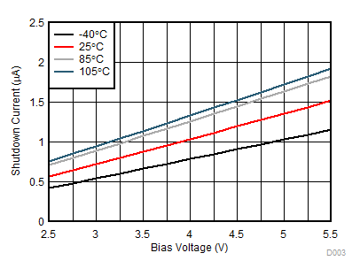
VIN1 = VIN2 = VBIASVON1 = VON2 = 0 VVOUT = 0 V
Figure 6-5 VBIAS Shutdown Current vs Bias Voltage Both Channels
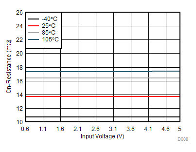
GUID-20231117-SS0I-HXVW-SDHN-MMQBVXXGTCXJ-low.svg
VBIAS = 5 V IOUT = –200 mA VON = 5 V
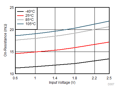
Figure 6-7 On-Resistance vs Input Voltage Single Channel - Across Ambient Temperatures (TPS22976)
GUID-20231117-SS0I-RN9V-6BJK-SZ4R0CRJBFBX-low.svg
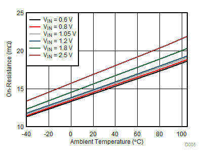
VBIAS = 5 V IOUT = –200 mA VON = 5 V
Figure 6-9 On-Resistance vs Ambient Temperature Single Channel (TPS22976)
GUID-74A0BA31-778B-45FB-BAA0-2EE77AF706F0-low.gif
VBIAS = 2.5 V IOUT = –200 mA VON = 5 V
Figure 6-11 On-Resistance vs Ambient Temperature Single Channel (TPS22976A, TPS22976N)
GUID-C66FB257-1B83-4F07-8C11-B39297E2C183-low.gif
VBIAS = 2.5 V IOUT = –200 mA VON = 5 V
Figure 6-13 On-Resistance vs Input Voltage Single Channel - Across Ambient Temperatures (TPS22976A, TPS22976N)
GUID-45D8C4E9-A163-4361-9105-40FEB724C907-low.gif
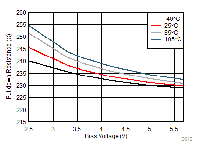
VIN = 2.5 VVON = 0 V
Figure 6-15 Pulldown Resistance vs Bias Voltage Single Channel
GUID-3D21CE61-A56D-4354-B07D-FE30E71225B8-low.gif
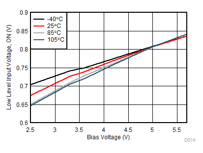
VIN = VBIAS
Figure 6-17 Low-Level Input Voltage vs Bias Voltage
GUID-8EA719BB-2306-48A3-BECC-03152C2D35F1-low.gif
VIN1 = VBIASVON1 = 5 VVOUT = Open
Figure 6-2 VBIAS Quiescent Current vs Bias Voltage Single Channel (TPS22976, TPS22976N)
GUID-20200920-CA0I-4R9K-C9TJ-SQJPM1W7X2R9-low.gif
VIN1 = VBIAS VON1 = 5 V VOUT = Open
Figure 6-4 VBIAS Quiescent Current vs Bias Voltage Single Channel (TPS22976A)
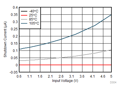
GUID-7FE04A8F-2C1C-4835-A6CE-C9F9661044A1-low.gif
VBIAS = 5 VVON = 0 VVOUT = 0 V
Note:–40°C and 25°C curves have similar values, therefore only one line is visible.
Figure 6-6 Off-State VIN Current vs Input Voltage Single Channel
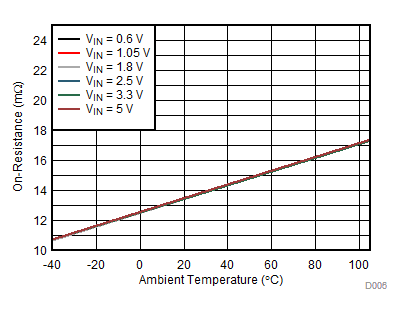
GUID-20231117-SS0I-RNZT-BSHF-JSKNCXVBJXVV-low.svg
VBIAS = 2.5 V IOUT = –200 mA VON = 5 V
Figure 6-8 On-Resistance vs Input Voltage Single Channel - Across Ambient Temperatures (TPS22976)
GUID-20231117-SS0I-LXV5-JF1J-PPNL0GW7VXMM-low.svg
VBIAS = 2.5 V IOUT = –200 mA VON = 5 V
Figure 6-10 On-Resistance vs Ambient Temperature Single Channel (TPS22976)
GUID-8B85E434-9E83-4483-B5AE-EF2E0835F5E0-low.gif
VBIAS = 5 V IOUT = –200 mA VON = 5 V
Figure 6-12 On-Resistance vs Ambient Temperature Single Channel (TPS22976A, TPS22976N)
GUID-C464B84E-5C43-41A3-A53C-8BAAEC3B27E1-low.gif
VBIAS = 5 V IOUT = –200 mA VON = 5 V
Figure 6-14 On-Resistance vs Input Voltage Single Channel - Across Ambient Temperatures (TPS22976A, TPS22976N)
GUID-6784B3A9-9733-4E78-B143-718B8C3138BF-low.gif
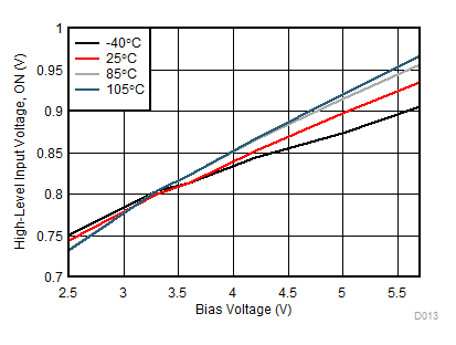
VIN = VBIAS
Figure 6-16 High-Level Input Voltage vs Bias Voltage
GUID-1AC346FF-EC8F-4F1C-9DE5-13DA1623653A-low.gif
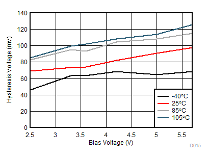
VIN = VBIAS
Figure 6-18 Voltage Input Hysteresis vs Bias Voltage