9.2.2 Detailed Design Procedure
9.2.2.1 Selecting RSNS
Before selecting RSNS, first compute the maximum load current. For this example the worst case load current happens at the minimum input voltage of 38 V. Thus the maximum current is 400 W/38 V = 10.5 A. To provide some margin, set the target current limit to 12 A and compute RSNS using equation below:
Equation 11. 
Use next available RSNS of 2 mΩ.
9.2.2.2 Selecting Soft Start Setting: CSS and CSS,VEE
First, compute the minimum inrush current where the timer will trip using equation below.
Equation 12. 
To avoid running the timer the inrush current needs to be sufficiently low. Target 0.4 A of inrush current to allow margin, and compute the target CSS using equation below.
Equation 13. 
Next choose, the next available CSS greater than 39.6 nF. For this example 43 nF was used, which assumes a 33 nF and 10 nF cap in parallel. This results in an inrush current of 0.37 A at max COUT (792 µF) and inrush current of 0.31 A at typical COUT (660 µF). Also it is recommended to add a capacitor between the soft start pin and VEE (CSS,VEE) to improve immunity to input voltage noise during soft start. It's recommended to chose a capacitor that's 3x larger than CSS. In this case a 150 nF capacitor was chosen.
Finally the start-up time at maximum input voltage can be computed using the equation below:
Equation 14. 
9.2.2.3 Selecting VDS Switch Over Threshold
The VDS threshold where the current limit switches from CL1 to CL2 can be programmed using RD. In general a higher threshold improves ability to ride through voltage steps, brown outs, and other transients. However, a larger setting can also expose the MOSFET to more stress, because the larger current limit is now allowed at higher VDS voltages. If there are no specific voltage step requirements, 20 V is a good starting point. Use the equation below to compute the target RD.
Equation 15. 
9.2.2.4 Timer Selection
The timer determines how long the hot swap can be in current limit before timing out and can be programmed using CTMR. In general a longer time out (TTO) improves ability to ride through voltage steps, brown outs, and other transients. However, a larger setting can also expose the MOSFET to more stress, because it takes longer for the FET to shut down during fault conditions. If there are no specific voltage step or transient requirements, 2 ms is a good starting point. Use the equation below to compute the target CTMR. Choose the next available capacitor value of 15 nF, which results in a 2.25 ms time out.
Equation 16. 
9.2.2.5 MOSFET Selection and SOA Checks
When selecting MOSFETs for the –48 V application the three key parameters are: VDS rating, RDSON, and safe operating area (SOA). For this application the CSD19535KTT was selected to provide a 100 V VDS rating, low RDSON, and sufficient SOA. After selecting the MOSFET, it is important to double check that it has sufficient SOA to handle the key stress scenarios: start-up, output Hot Short, and Start into Short. MOSFET's SOA is usually specified at a case temperature of 25°C and should be derated based on the maximum case temperature expected in the application. Compute the maximum case temperature using the equation below. Note that the RDSON will vary with temperature and solving the equation below could be a repetitive process. The CSD19535KTT, has a maximum 3.4 mΩ RDSON at room temperature and is ~1.5x higher at 100°C. N stands for the number of MOSFETs used in parallel.
Equation 17. 
Equation 18. 
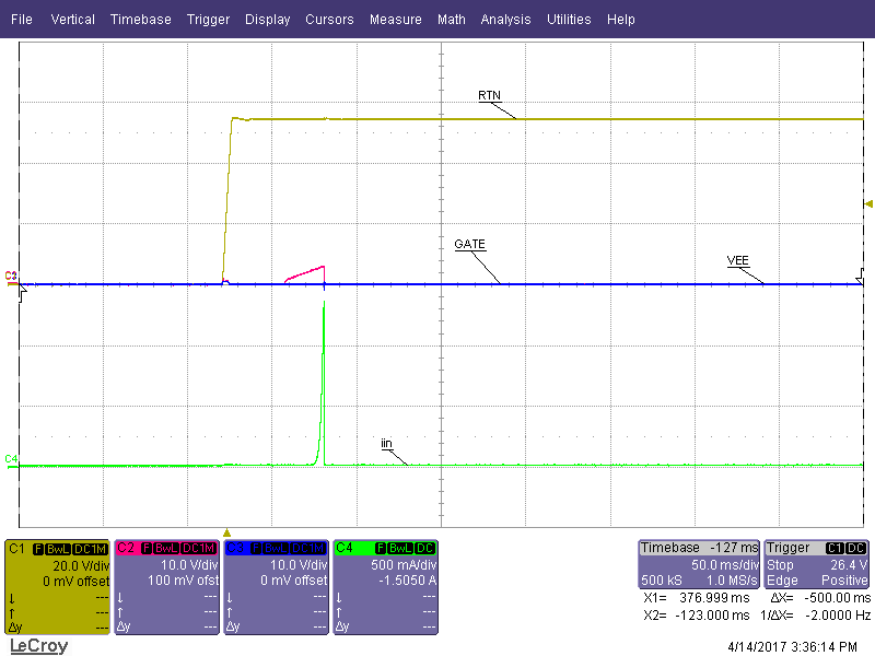
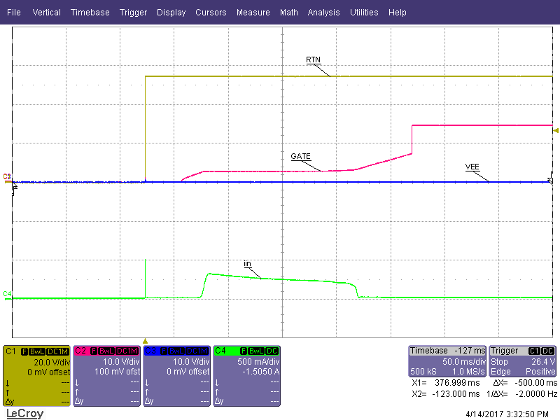
Next the stress the MOSFET will experience during operation should be compared to the FETs capability. First, consider the power up. The inrush current with max COUT will be 0.37 A and the inrush will last for 129 ms. Note that the power dissipation of the FET will start at VIN,MAX × IINR and reduce to zero as the VDS of the MOSFET is reduced. The SOA curve of a typical MOSFET assume the same power dissipation for a given time. A conservative approach is to assume an equivalent power profile where PFET = VIN,MAX × IINR for t = Tstart-up /2. In this instance, the SOA can be checked by looking at a 60 V, 0.4 A, 64.5 ms pulse. Based on the SOA of the CSD19535KTT, it can handle 60 V, 1.8 A for 10 ms and it can handle 60 V, 1 A for 100 ms. The SOA at TC = 25°C for 64.5 ms can be extrapolated by approximating SOA vs time as a power function as shown in equations below:
Equation 19. 
Equation 20. 
Equation 21. 
Equation 22. 
Finally, the FET SOA needs to be derated based on the maximum case temperature as shown below. Note that the FET can handle 0.59 A, while it will have 0.37 A during start-up. Thus there is a lot of margin during this test condition.
Equation 23. 
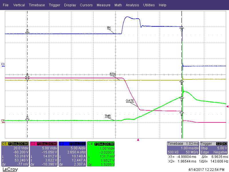
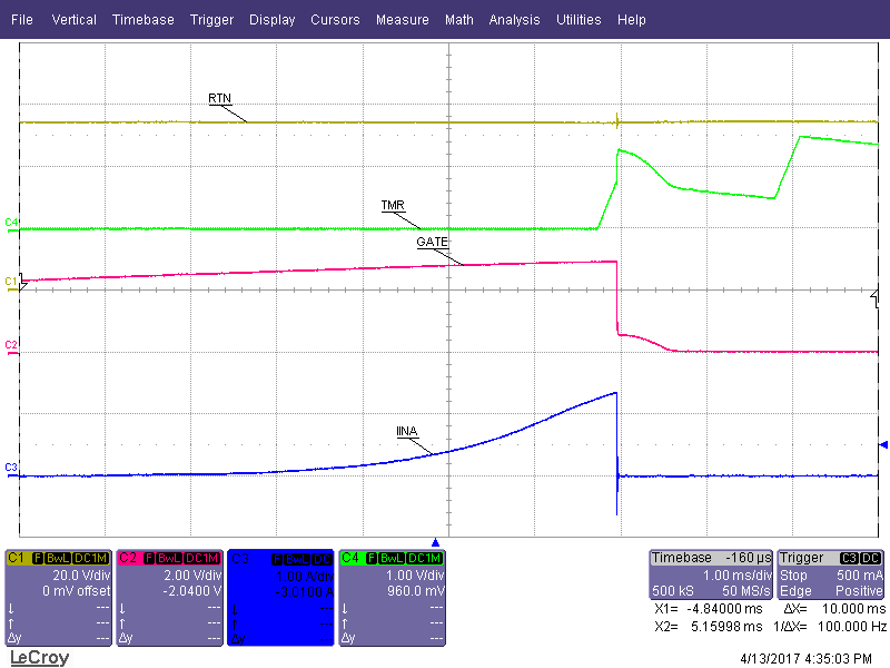
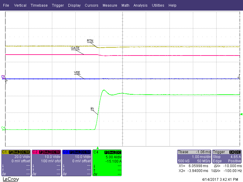
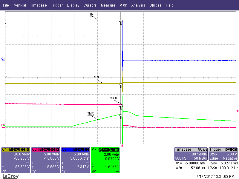
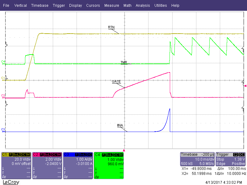
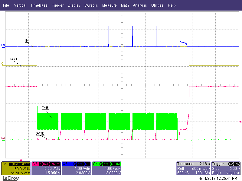
A similar approach should be taken to compute the FETs SOA capability during a Hot Short and start into short. As shown in the following figure, during a start into short the gate is coming up very slowly due to a large capacitance tied to the gate through the SS pin. Thus it is more stressful than a Hot Short and should be used for worst case SOA calculations. To compare the FET stress during start-up into short to the SOA curves the stress needs to be approximated as a square pulse as showing in the figure below. In this example, the stress is approximated with a 1.1 ms (Teq), 1.5 A, 60 V pulse. The FET can handle 6 A, 60 V for 1 ms and 1.8 A, 60 V for 10 ms. Using approximation and temp derating as shown earlier, the FET's capability can be computed as 3 A, 60 V, for 1.1 ms at 96°C. 3 A is significantly larger than 1.5 A implying good margin.
The final operating point to check is the operation with high current and VDS just below the VDS,SW threshold. In this example, the time out would be 1.1ms (one half of the time out at Vd = 0 V), the current will be 12.5 A, and the voltage would be 20 V. Looking up the SOA curve, the FET can handle 30 A, 20 V for 1 ms and 10 A, 20 V for 10 ms. Repeating previously shown approximations and temp derating, the FET's capability is computed to be 16 A, 20 V, for 1.1 ms at 96°C. Again this is below the worst case operating point of 12.5 A and 20 V suggesting good margin.
9.2.2.6 Input Cap, Input TVS, and OR-ing FET selection
This design example is sized for an application that needs to pass a 2 kV, 2Ω lightning strike per IEC61000-4-5. This equates to almost 1000 A of input current that needs to be clamped. In addition, the design needs to pass reverse hook up and thus the TVS needs to be bi directional. A ceramic transient voltage suppressor (2x B72540T6500S162) CT2220K50E2G was used to clamp this huge surge of current. According to it's datasheet it can clamp 500 A of current to 150 V. Note that the lightning strike can be positive or negative. The worst case voltage is dropped across the OR-ing FETs when the strike is positive (–48 V line goes above RTN). If the output of the OR-ing is –48 V and the input goes to +150 V that is a 200 V drop. Thus BSC320N20NS3 was chosen for the OR-ing FETs. This is a 200 V FET with a 32 mΩ RDSON at room temperature. 2 of these were used in parallel to minimize power loss and manage thermal. Finally a 0.1 µF input bypass cap is recommended.
9.2.2.7 EMI Filter Consideration
In this example it is assumed that the EMI filter is right after the hot swap and the bulk cap is after the EMI filter. The EMI filter adds significant inductance and needs to be accounted for. During a Hot Short, the inductor builds up significant current that needs to go somewhere after the FET opens. For that a free wheeling diode should be used along with a snubber. For this example a 150 V, SMA diode was used: STPS1150A. The snubber consisted of a 10-Ω resistor in series with a 1-µF ceramic capacitor. In addition a 0.1-µF ceramic cap was tied directly on the output.
9.2.2.8 Under Voltage and Over Voltage Settings
Both the threshold and hysteresis can be programmed for under voltage and over voltage protection. In general the rising UV threshold should be set sufficiently below the minimum input voltage and the falling OV threshold should be set sufficiently above the maximum input voltage to account for tolerances. For this example a rising UV threshold of 37 V and a falling UV threshold of 35 V was chosen as the target. First, choose RUV1 based on the 2 V UV hysteresis as shown below.
Equation 24. 
Once RUV1 is known RUV2 can be computed based on the target rising UV threshold as shown below.
Equation 25. 
The OV setting can be programmed in a similar fashion as shown in equations below.
Equation 26. 
Equation 27.
Equation 28. 
Optional filtering capacitors can be added to the UV and OV to improve immunity to noise and transients on the input bus. These should be tuned based on system requirements and input inductance. In this example place holders were added to the PCB, but the components were not populated.
9.2.2.9 Choosing RVCC and CVCC
The VCC is used as internal supply rail and is a shunt regulator. To ensure stability of internal loop a minimum of 0.1 µF is required for CVCC. To ensure reasonable power on time it is recommended to keep CVCC below 1 µF. RVCC should be sized in such a way to ensure that sufficient current is supplied to the IC at minimum operating voltage corresponding to the falling UV threshold. To allow for some margin it is recommended that the current through RVCC is at least 1.2x of IQ,MAX when RTN = Falling UV threshold and VCC = 10 V (minimum recommended operating voltage on VCC). For this example RVCC of 16.2 kΩ was used.
9.2.2.10 Power Good Interface to Downstream DC/DC
It's critical to keep the downstream DC/DC off while the hot swap is charging the bulk capacitor. This can be accomplished through the PGb pin. Note that the VEE of the hot swap and the DC/DC are different and the Power Good can not be directly tied to the EN or UV of the DC/DC. The application circuit below provides a simple way to control the downstream converter with the PGb pin of the hot swap.
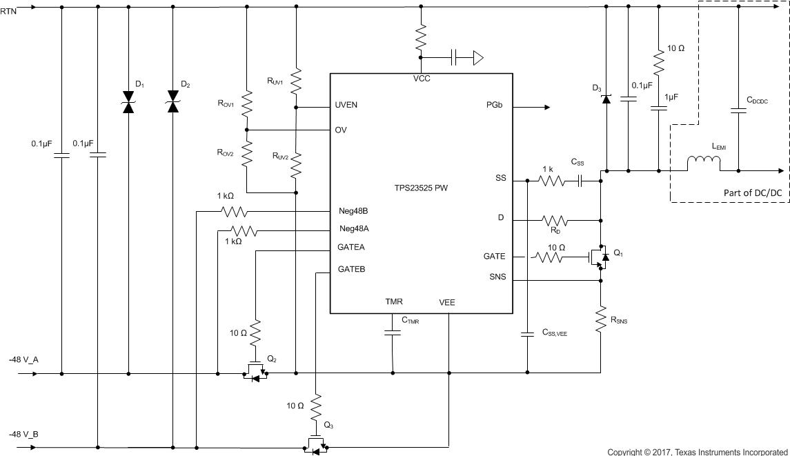 Figure 12. Application Diagram for Design Example


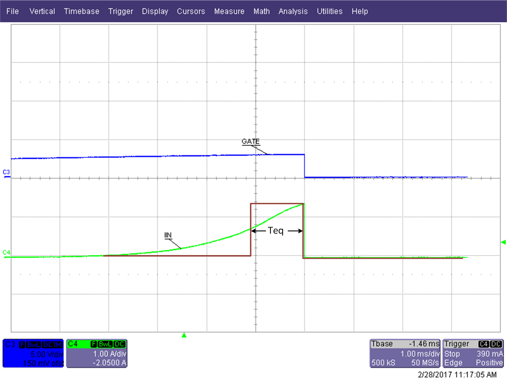 Figure 13. Teq During a Start Into a Short


 Figure 14. Interface to DC/DC


